Display substrate and display device
A technology for display substrates and display areas, applied in identification devices, organic semiconductor devices, photovoltaic power generation, etc., can solve problems such as differences in display effects, achieve the effect of solving stress concentration and ensuring display effects
- Summary
- Abstract
- Description
- Claims
- Application Information
AI Technical Summary
Problems solved by technology
Method used
Image
Examples
Embodiment 1
[0039] This embodiment provides a display substrate, which can effectively solve the problem of display differences caused by deformation of openings in the display area.
[0040] A display substrate, including a substrate, the substrate at least includes a display area, the substrate forms a plurality of islands separated by openings and connected by bridges in the display area, and the substrates in at least two different areas of the display area have different modulus of elasticity. By dividing the display area of the substrate into different areas and adjusting the elastic modulus for different areas, the accumulated deformation of the central area of the display area is reduced, and the deformation difference between the central area and the edge area of the display area is eliminated.
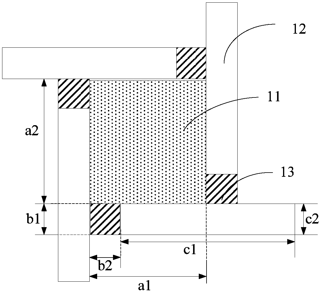
[0041] When partitioning the display area, the substrate can be divided into different opening areas along a certain direction of pixel arrangement in the display area (for example...
Embodiment 2
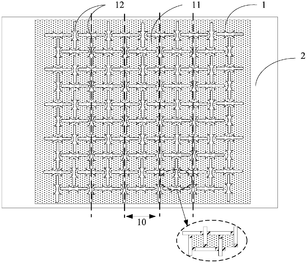
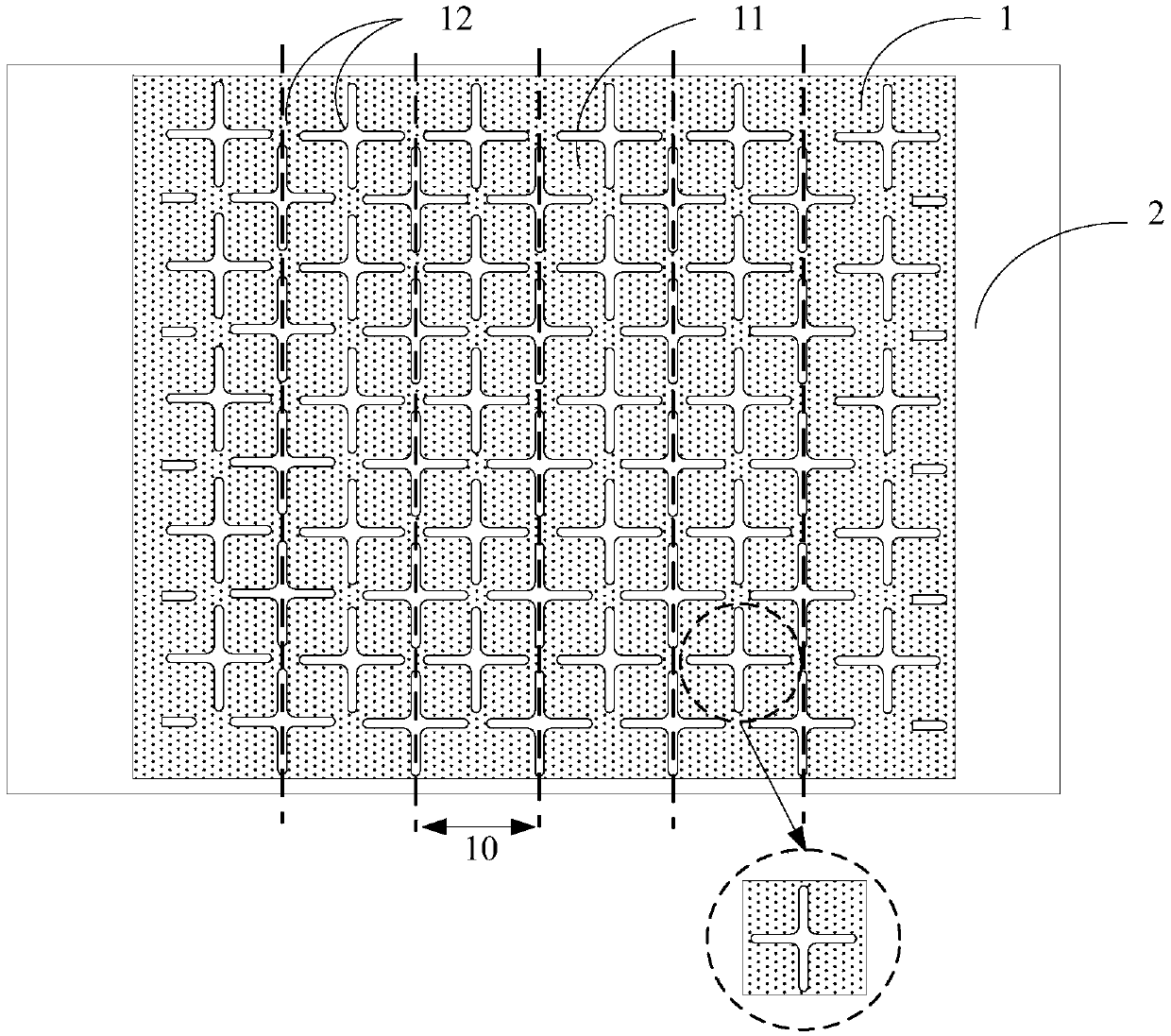
[0045] Usually, due to the difference in the surrounding structure of the display area, the stretchable deformation is in two directions perpendicular to each other (for example image 3 , Figure 4 The illustrated transverse direction X and longitudinal direction Y) have different situations. Such as Figure 1A As shown, the substrate also includes two non-display areas 2 located on opposite sides of the display area 1 , the substrate is divided into a plurality of opening areas 10 in the display area 1 , and different opening areas 10 have different elastic moduli.
[0046] Figure 1AIn this method, different opening regions 10 are arranged in the same direction, and the substrate is alternately arranged with the first elastic modulus and the second elastic modulus in the plurality of opening regions 10, and the first elastic modulus is not equal to the second elastic modulus. That is to say, the two sides of the region with a smaller modulus of elasticity are regions with ...
Embodiment 3
[0061] On the basis of Embodiment 1, the display substrate in this embodiment also adopts pixel compensation on the basis of hole structure compensation. By setting different pitches between pixels, a pre-compensation is applied before stretching the substrate to reduce the pitch difference between pixels on the substrate after stretching, so as to solve the problem of display differences caused by different pixel pitches .
[0062] For different pixel compensations, if the opening widths in the E1 area and E2 area are different, the distance between adjacent islands is different before stretching, and the deformation of the opening is also different after the force is applied, driving the distance between pixels to tend to same. In practical applications, when performing pixel compensation for this situation, it is necessary to consider the deformation result of the combination of the elastic modulus of the opening area and the initial pixel spacing.
[0063] In one embodim...
PUM
 Abstract
Description
Claims
Application Information


