High-voltage LED flip-chip and method for forming same

An LED chip and flip-chip technology, applied in electrical components, circuits, semiconductor devices, etc., can solve the problems of high-voltage flip-chip LED chip leakage failure, puncture of the insulating protective layer, etc.

Inactive Publication Date: 2019-05-07
ENRAYTEK OPTOELECTRONICS
View PDF9 Cites 3 Cited by
  • Summary
  • Abstract
  • Description
  • Claims
  • Application Information

AI Technical Summary

Problems solved by technology

[0006] The purpose of the present invention is to provide a high-voltage flip-chip LED chip and its forming method, which is used to solve the problem that the thimble is easy to stab the side insulating protection layer at the Mesa table in the isolation area, thereby causing the leakage of the high-voltage flip-chip LED chip failure problem

Method used


Image

  • High-voltage LED flip-chip and method for forming same
  • High-voltage LED flip-chip and method for forming same
  • High-voltage LED flip-chip and method for forming same

Examples


Embodiment Construction

[0023] The specific implementation manner of the present invention will be described in more detail below with reference to schematic diagrams. Advantages and features of the present invention will be apparent from the following description and claims. It should be noted that all the drawings are in a very simplified form and use imprecise scales, and are only used to facilitate and clearly assist the purpose of illustrating the embodiments of the present invention.

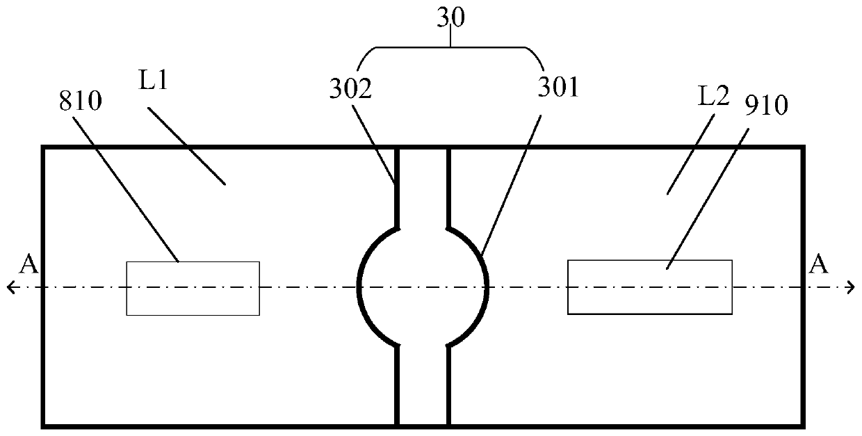
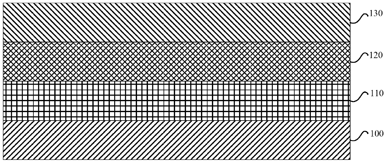
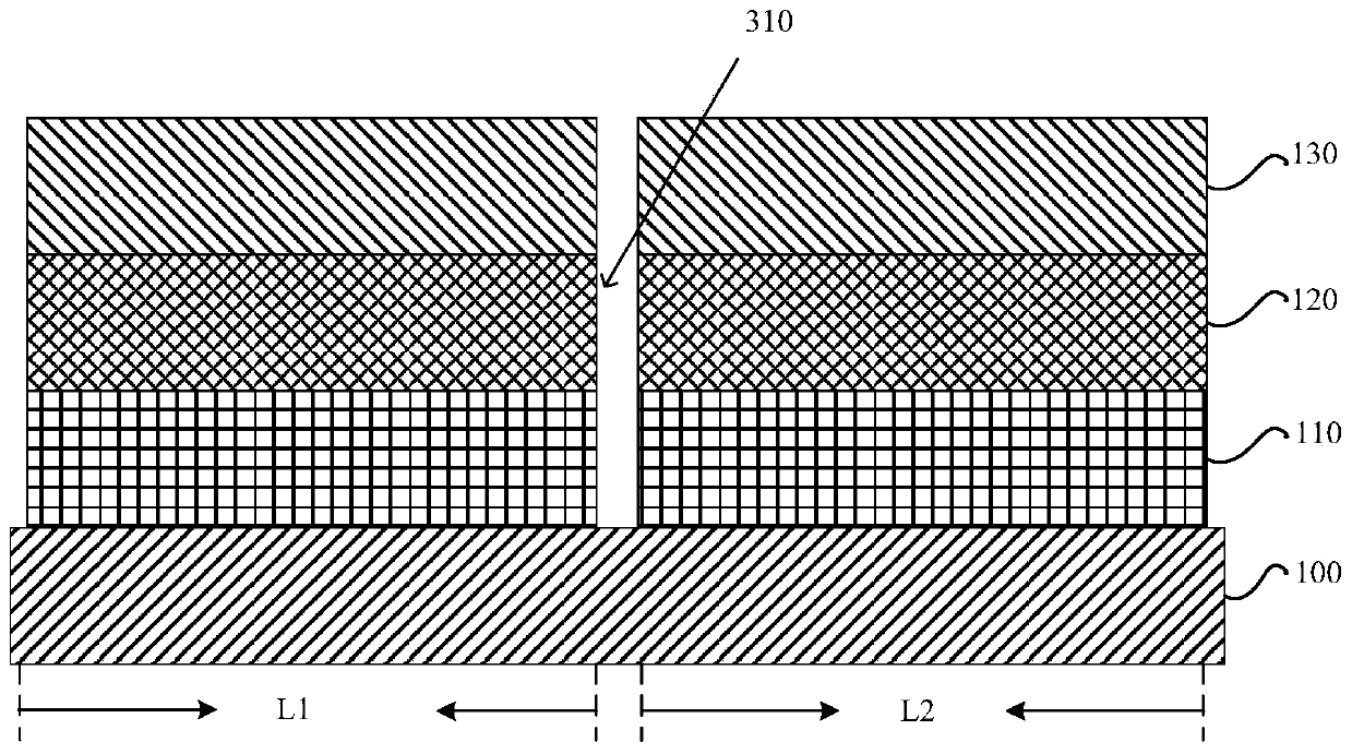
[0024] Such as figure 1 As shown, a high-voltage flip-chip LED chip provided in this embodiment includes: at least two light-emitting units connected in series and / or in parallel, and two adjacent light-emitting units are isolated by a trench isolation structure 30, located at The center of the high-voltage flip-chip LED chip or the area on the upper surface of the trench isolation structure 30 where the thimble passes is the isolation region. The high-voltage flip-chip LED chip is in the shape of a cube as a w...


PUM

PropertyMeasurementUnit
Diameteraaaaaaaaaa

Abstract

The invention discloses a high-voltage LED flip-chip and a method for forming the same. The chip comprises at least two interconnected light-emitting units; a plurality of trench isolation structureseach of which is used for isolating two adjacent light-emitting unit, wherein the inner surface of each trench isolation structure is covered with an insulating protective layer; at least one trench isolation structure passes through the central axis of the high-voltage LED flip-chip; the trench isolation structure passing through the central axis includes an outer expanded segment and a trench section, the trench section communicates with the outer expanded section, and the outer expanded section comprises a thimble area. The method solves the problem that the thimble punctures the insulatingprotective layer on the trench isolation structure, thereby causing the electric leakage of the high-voltage LED flip-chip.

Description

technical field [0001] The invention relates to the technical field of LED manufacturing, in particular to a high-voltage flip-chip LED chip and a forming method thereof. Background technique [0002] A light-emitting diode (LED, Light Emitting Diode) is a semiconductor solid-state light-emitting device, which uses a semiconductor PN junction as a light-emitting material, and can convert electricity into light. When a forward voltage is applied to both ends of the semiconductor PN junction, the electrons and holes injected into the PN junction recombine, and the excess energy is released in the form of photons. LEDs have the advantages of long life and low power consumption. With the maturity of technology, the application fields of LEDs are becoming more and more diversified, and the requirements for the power and brightness of LED chips are also getting higher and higher. [0003] At present, as a solution to high-power LEDs, high-voltage LED chips (High Voltage LEDs, HVL...

Claims


Application Information

Patent Timeline
IPC IPC(8): H01L33/06H01L33/32H01L33/08H01L33/20H01L33/44H01L33/00
Inventor 沈铭
Owner ENRAYTEK OPTOELECTRONICS
Why Eureka
Try Eureka