Display substrate, preparation method thereof and display device

A technology for display substrates and substrate substrates, which is applied in the manufacture of semiconductor/solid-state devices, diodes, organic semiconductor devices, etc., and can solve the problems of color separation of display substrates

Active Publication Date: 2019-05-07
BOE TECH GRP CO LTD +1
View PDF5 Cites 3 Cited by
  • Summary
  • Abstract
  • Description
  • Claims
  • Application Information

AI Technical Summary

Problems solved by technology

[0006] Embodiments of the present invention provide a display substrate, a preparation method thereof, an

Method used


Image

  • Display substrate, preparation method thereof and display device
  • Display substrate, preparation method thereof and display device
  • Display substrate, preparation method thereof and display device

Examples


no. 1 example

[0041] The invention provides a display substrate.

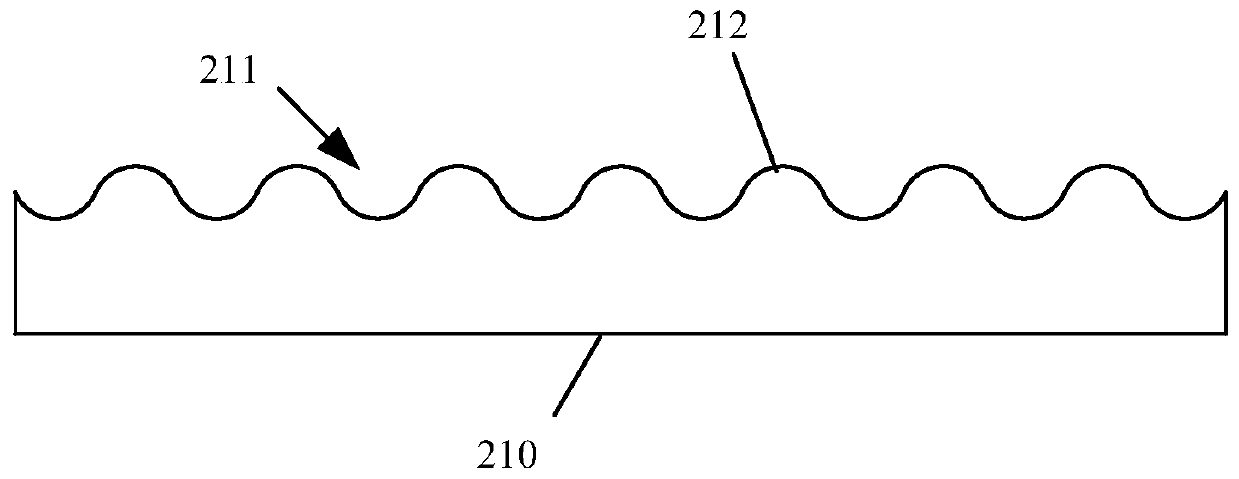
[0042] Such as Figure 3 to Figure 7 As shown, in one embodiment, the display substrate includes a planarization layer 210 (Planarization, PLN for short) on the base substrate and a first electrode layer 220 on the planarization layer 210 .

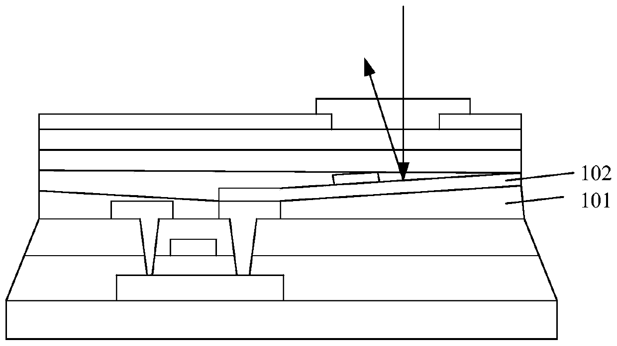
[0043] It should be understood that the flat layer 210 may not be directly formed on the base substrate, and there may be some other functional film layers between the flat layer 210 and the base substrate. For details, please refer to the existing and possible display substrates, It will not be further defined and described here.

[0044] The side of the flat layer 210 away from the base substrate includes a scattering structure, the first electrode layer 220 is located on the scattering structure, and the thickness of the first electrode layer 220 is uniform everywhere, which can also be understood as the thickness of the first electrode layer 220 everywhere. are basically equal.

...

no. 2 example

[0067] This embodiment provides a display device, including any one of the above-mentioned display substrates. Since the technical solution of this embodiment includes all the technical solutions of the above-mentioned embodiments, at least all the above-mentioned technical effects can be achieved, and details will not be repeated here.

[0068] Further, the display device may include but not limited to mobile phones, tablet computers, e-book readers, MP3 players, MP4 players, digital cameras, laptop computers, vehicle-mounted computers, desktop computers, set-top boxes, smart TVs, At least one of the wearable devices.

no. 3 example

[0070] This embodiment provides a method for preparing a display substrate.

[0071] Such as Figure 8 As shown, the preparation method of the display substrate includes:

[0072] Step 801: forming a flat layer 210 on the base substrate; and

[0073] The first electrode layer 220 is formed on the planarization layer 210 .

[0074] The above step 801 can refer to the existing process of forming the flat layer 210, and before forming the flat layer 210, some other functional film layers may also be formed, that is, the flat layer 210 may not be directly formed on the surface of the substrate, but It is to first form some other functional film layers on the base substrate, and then form the planar layer 210 on these functional film layers, these functional film layers include but not limited to gate layer, gate insulating layer, active layer, source-drain For the functional film layers such as the electrode layer, reference may be made to existing possible display substrates, ...


PUM


Abstract

The invention provides a display substrate, a preparation method thereof and a display device. The display substrate comprises a flat layer positioned on a substrate and a first electrode layer positioned on the flat layer, the side, far from the substrate, of the flat layer comprises a scattering structure, the first electrode layer is positioned on the scattering structure, and the thickness indifferent positions of the first electrode layer is the same. When light is input to the first electrode layer via a color filter in a packaging layer, the shape of the first electrode layer is basically the same with that of the scattering structure due to existence of the scattering structure, the incident light is scattered in the first electrode layer, and thus, red, green and blue light reflected by anodes of red, green and blue pixels can be scattered to different direction relatively uniformly, and a color separation phenomenon can be weakened or eliminated effectively.

Description

technical field [0001] The invention relates to the field of display technology, in particular to a display substrate, a preparation method thereof, and a display device. Background technique [0002] The color separation phenomenon of the color filter refers to that when the incident light from the color filter (Color Filter, CF for short) of the display substrate is reflected by pixels of different colors, due to the different inclination angles of different pixels, the incident light Scattering occurs. [0003] Specifically, such as figure 1 As shown, when a hole is drilled on the flat layer (PLN) 101 , the thickness of the flat layer 101 around the hole will change, so the flat layer 101 will form a slope, thereby causing the anode 102 formed on the flat layer 101 to tilt. In addition, if figure 2 As shown, factors such as the routing of the source and drain electrodes 103 (Source & Drain, S / D for short) may also cause the anodes corresponding to pixels of different ...

Claims


Application Information

Patent Timeline
IPC IPC(8): H01L51/52H01L27/32H01L21/77
CPCH01L21/77H10K59/35H10K59/38H10K50/813H10K50/854H10K2102/351H10K59/353H10K50/84H10K71/00
Inventor 唐国强胡耀汪杨鹏
Owner BOE TECH GRP CO LTD
Why Eureka
Try Eureka