Tunable hyperspectral infrared detector and detection function structure, hyperspectral imaging equipment
An infrared detector and functional structure technology, applied in the field of infrared light detection, can solve the problems that thermal infrared band cannot be applied, and can only cover the band range from visible light to short-wave infrared.
- Summary
- Abstract
- Description
- Claims
- Application Information
AI Technical Summary
Problems solved by technology
Method used
Image
Examples
Embodiment 1
[0047] see figure 1 , is a schematic structural diagram of an embodiment of a conductive graphene plasmon-based tunable hyperspectral infrared detector of the present invention, specifically, the tunable hyperspectral infrared detector of this embodiment includes a detection function Structure, which includes from top to bottom:
[0048] The electrode layer, specifically, the electrode layer includes a first electrode 201 and a second electrode 202. In a specific embodiment, the first electrode 201 and the second electrode 202 are made of gold with a thickness of 80nm, which can The size of the tuned hyperspectral infrared detector is 100 μm × 100 μm, and the size is 100 μm × 15 μ. Further, in order to enhance the adhesion of the electrode layer, chromium with a thickness of 5 nm is added under the first electrode and the second electrode;
[0049] Graphene layer 203, specifically, the graphene layer adopts double-layer graphene, and each layer of graphene is continuous graph...
Embodiment 2
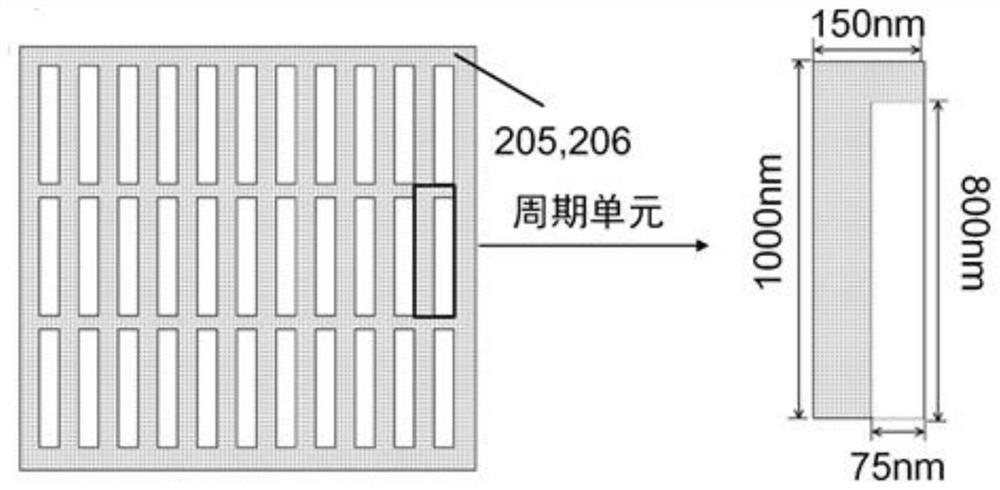
[0055] The present invention also provides another tunable hyperspectral infrared detector based on conductive graphene plasmons. The tunable hyperspectral infrared detector of this embodiment includes each structure in the above-mentioned embodiment 1, different Yes, the first conductive periodic scatterer and the second conductive periodic scatterer in the tunable hyperspectral infrared detector in this embodiment both use a one-dimensional conductive grating.
[0056] In a specific embodiment, the period of the one-dimensional conductive grating is 80 nm, the thickness is 100 nm, and its material is graphene.
[0057] Of course, the first conductive periodic scatterer can also use a one-dimensional conductive grating, and the second conductive periodic scatterer can use a two-dimensional conductive grating; or the second conductive periodic scatterer can use a one-dimensional conductive grating, and the second conductive periodic The scatterer adopts a one-dimensional condu...
Embodiment 3
[0059] see Figure 4 , is a structural schematic diagram of another embodiment of a conductive graphene plasmon-based tunable hyperspectral infrared detector of the present invention, the tunable hyperspectral infrared detector of this embodiment includes the above-mentioned embodiment 1 or each structure in 2, the difference is that the tunable hyperspectral infrared detector in this embodiment also includes a reflection enhancement structure arranged under the detection function structure, specifically, the reflection enhancement structure includes calcium fluoride A dielectric layer 207 with a thickness of 1.5 um and a reflective layer 208 located under the dielectric layer are produced. Specifically, the reflective layer 208 is made of gold with a thickness of 200 nm.
[0060] Further, in this embodiment, an adhesion layer may also be provided under the reflective layer, specifically, it is made of 5nm chrome.
PUM
| Property | Measurement | Unit |
|---|---|---|
| thickness | aaaaa | aaaaa |
| thickness | aaaaa | aaaaa |
| thickness | aaaaa | aaaaa |
Abstract
Description
Claims
Application Information


