A contact type linear stress sensor and its stress detection method
A stress sensor and stress detection technology, which is applied in the measurement, instrumentation, and measurement force of the change force of the optical properties of the material when it is stressed, can solve the problems of light source attenuation, wavelength drift, and light source change in the measurement results.
- Summary
- Abstract
- Description
- Claims
- Application Information
AI Technical Summary
Problems solved by technology
Method used
Image
Examples
Embodiment 1
[0054] A contact-type linear stress sensor based on an arrayed waveguide grating structure, such as Figure 4 As shown, it includes an optical signal input module 11, an arrayed waveguide grating, and a spectral detection module 12 connected in sequence; the wide-spectrum optical signal input module 11 integrates a broadband halogen fiber optic illuminator, and its function is to provide a wide-spectrum light source for the sensor and detect spectral signals. A small CCD spectrometer is integrated inside the module 12, and its function is to detect the drift of the arrayed waveguide grating output spectrum;
[0055] The optical signal input module 11 is used to provide a wide-spectrum optical signal for stress detection, the arrayed waveguide grating is the contact area of the force-applying object, and the spectrum detection module 12 is used to detect the wavelength of the output signal.
Embodiment 2
[0057] According to the contact type linear stress sensor based on the arrayed waveguide grating structure described in Embodiment 1, the difference is that:
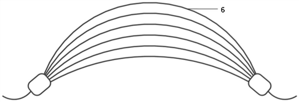
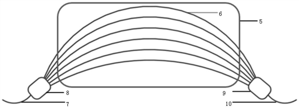
[0058] Such as figure 2 , image 3 As shown, the arrayed waveguide grating includes an input channel 7, an input slab waveguide 8, several single-mode waveguides 6, an output slab waveguide 9, and an output channel 10 connected in sequence; an optical signal input module 11 is connected to the input channel 7, and the output channel 10 is connected to the spectral A detection module 12; both ends of each single-mode waveguide 6 are respectively connected to the input slab waveguide 8 and the output slab waveguide 9;
[0059] The array area composed of several single-mode waveguides 6 is packaged into a rectangular area, which is used as the refractive index sensitive area 5, that is, the stress contact detection area;
[0060] The refractive index sensitive area 5 is the contact area of the force-applying object. ...
Embodiment 3
[0070] According to the contact type linear stress sensor based on the arrayed waveguide grating structure described in Embodiment 2, the difference is that the width of the single-mode waveguide 6 is 2 μm, and the thickness of the single-mode waveguide 6 is 1 μm.
PUM
| Property | Measurement | Unit |
|---|---|---|
| thickness | aaaaa | aaaaa |
| thickness | aaaaa | aaaaa |
| thickness | aaaaa | aaaaa |
Abstract
Description
Claims
Application Information


