Contact type linear stress sensor based on mini-ring structure and stress detection method thereof
A stress sensor, contact-type technology, applied in the measurement of the change force of its optical properties when the material is under stress, fluid pressure measurement using optical methods, instruments, etc., can solve problems such as the influence of changes, and achieve zero work low energy consumption, flexible usage scenarios, and simple process
- Summary
- Abstract
- Description
- Claims
- Application Information
AI Technical Summary
Problems solved by technology
Method used
Image
Examples
Embodiment 1
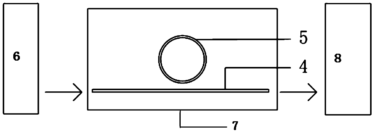
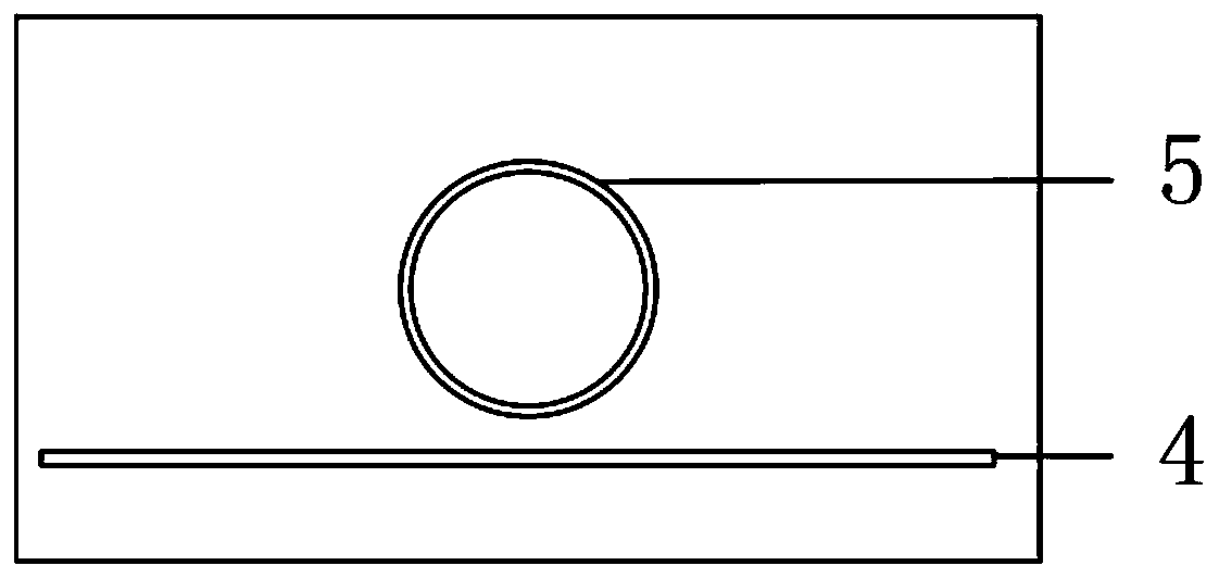
[0047] A contact-type linear stress sensor based on a microring structure, such as figure 2 , image 3 As shown, it includes a broadband light source 6, a microring resonant cavity 7, and a spectrum analyzer 8 connected in sequence;
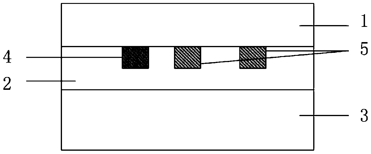
[0048] like figure 1 As shown, the microring resonator 7 sequentially includes a substrate 3, a lower confinement layer 2, a channel straight waveguide 4, a microring waveguide 5, and an upper confinement layer 1 from bottom to top;
[0049] The area where the channel straight waveguide 4 and the micro-ring waveguide 5 are located is the refractive index sensitive area, that is, the stress contact detection area;
[0050]After the signal light is input from the left port of the channel straight waveguide 4, mutual coupling occurs when it is adjacent to the microring resonator 7, so that part of the optical power input by the channel is continuously coupled into the microring resonator 7, and at the same time in the microring resonator 7 Part ...
Embodiment 2
[0053] According to the contact type linear stress sensor based on the microring structure described in Embodiment 1, the difference is that: the diffraction order of the microring resonant cavity 7 is m=50, and the center wavelength is 532 nm.
Embodiment 3
[0055] According to the contact type linear stress sensor based on the microring structure described in Embodiment 1, the difference is that there are two channel straight waveguides 4, forming parallel channel waveguides.
PUM
| Property | Measurement | Unit |
|---|---|---|
| thickness | aaaaa | aaaaa |
| thickness | aaaaa | aaaaa |
| wavelength | aaaaa | aaaaa |
Abstract
Description
Claims
Application Information
 - R&D
- Intellectual Property
- Life Sciences
- Materials
- Tech Scout
- Unparalleled Data Quality
- Higher Quality Content
- 60% Fewer Hallucinations
Browse by: Latest US Patents, China's latest patents, Technical Efficacy Thesaurus, Application Domain, Technology Topic, Popular Technical Reports.
© 2025 PatSnap. All rights reserved.Legal|Privacy policy|Modern Slavery Act Transparency Statement|Sitemap|About US| Contact US: help@patsnap.com


