Electronic device
An electronic device and fingerprint recognition technology, which is applied in the field of communication, can solve problems such as the inability to realize fingerprint recognition or accurate recognition, and achieve the effect of reducing light leakage
- Summary
- Abstract
- Description
- Claims
- Application Information
AI Technical Summary
Problems solved by technology
Method used
Image

Examples
Embodiment 1
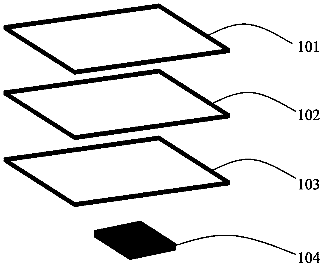
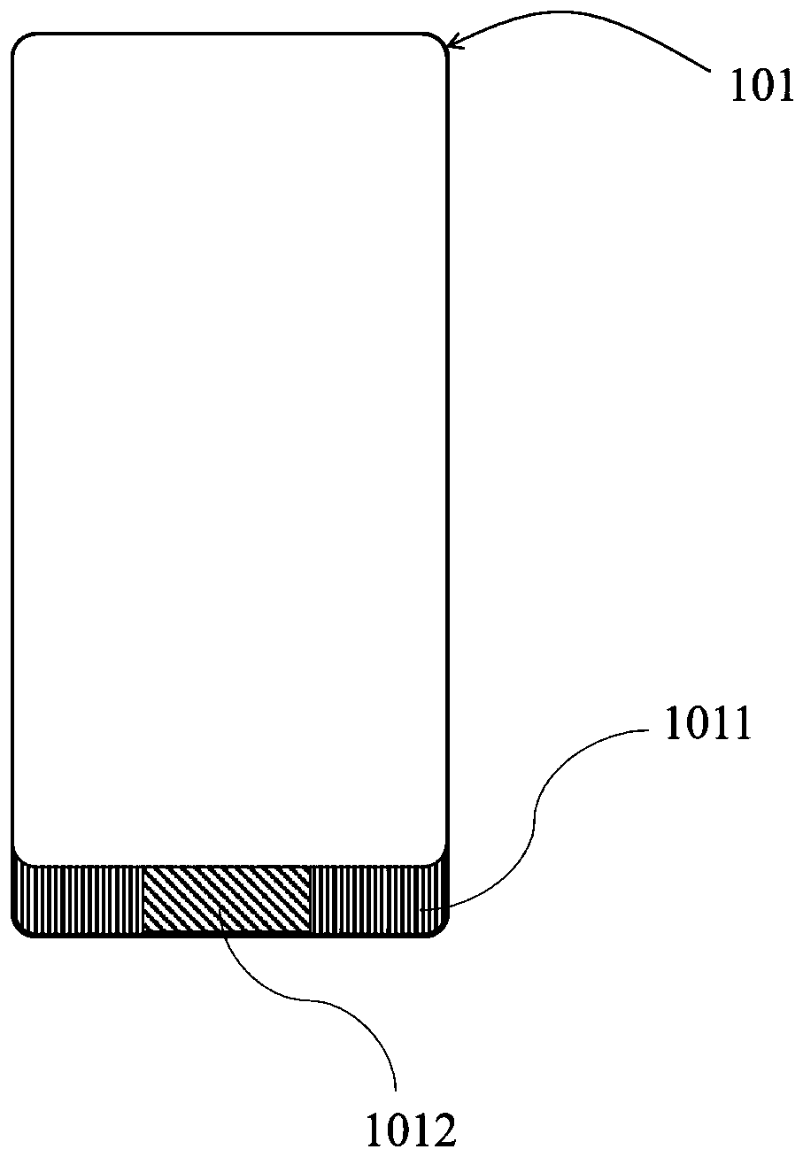
[0044] First, through Figure 2-5 , with regard to the electronic device of Embodiment 1 of the present invention, the glass cover plate 101, the LCD liquid crystal panel 102, the backlight module 103 and the fingerprint recognition sensor 104 which are stacked sequentially from top to bottom, and the backlight The infrared transparent shading layer 105 on the module 103; wherein, the glass cover plate 101 has a non-display area 1011, and the non-display area 1011 includes a fingerprint identification area 1012 (such as image 3 As shown), the fingerprint recognition area 1012 corresponds to the infrared transparent light-shielding layer 105 and the fingerprint recognition sensor 104. The infrared transparent light-shielding layer 105 can transmit infrared light but block visible light, so that the biological fingerprint infrared signal pass through the fingerprint recognition area 1012 and the infrared transparent light-shielding layer 105 , and be collected by the fingerprin...
Embodiment 2
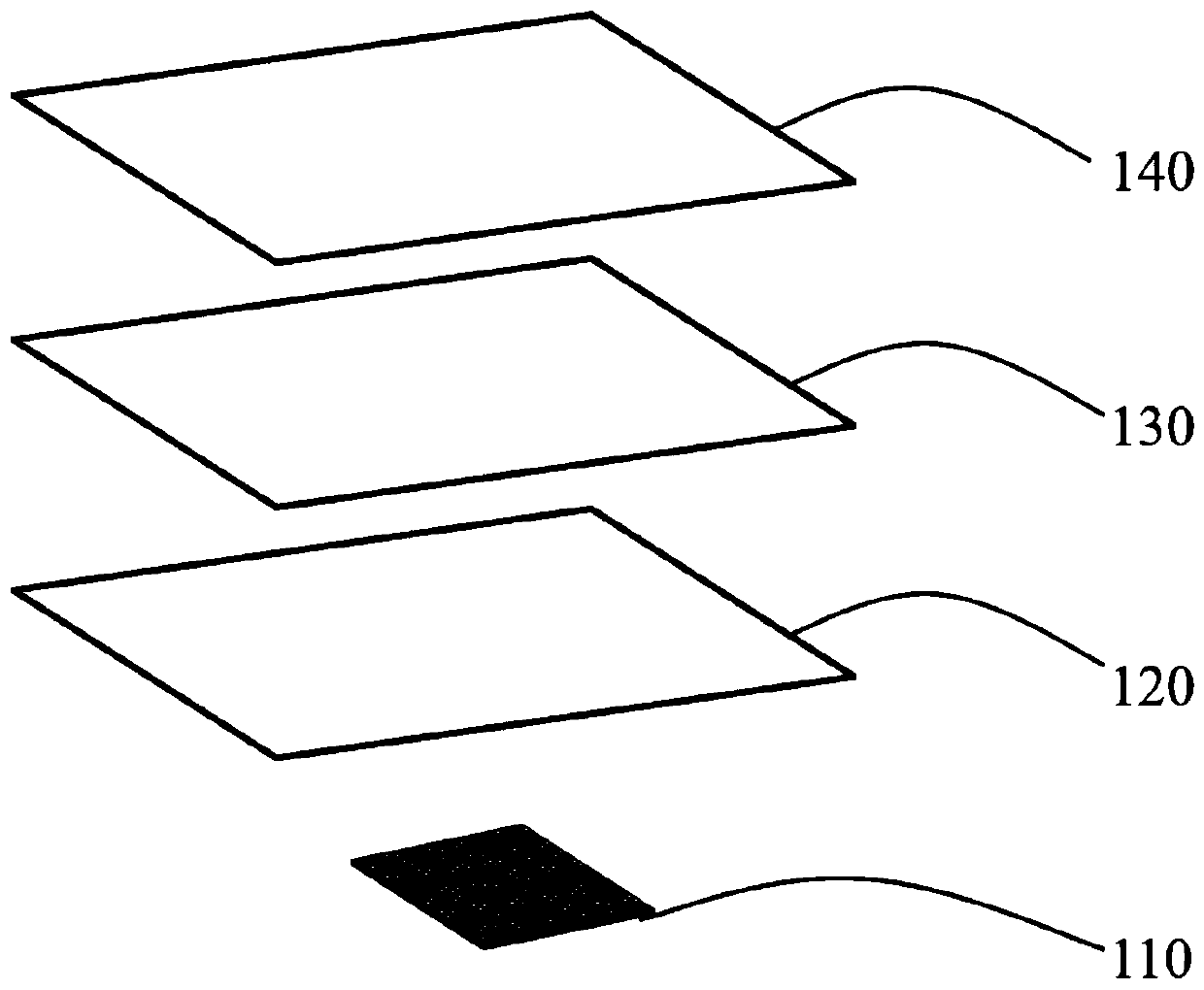
[0056] Please refer to Image 6 , is an exploded view of the electronic device according to Embodiment 2 of the present invention. Only the differences between Embodiment 2 and Embodiment 1 will be described below, and the similarities will not be repeated here.
[0057] The reflection sheet 240 , the light guide plate 230 , the diffusion film 220 , and the prism sheet 210 on the backlight module 103 are not provided with gaps. The light guide plate 230 is provided with a hollow area, and the vertical projection of the first overlapping area 1013 on the light guide plate 230 is included in the range of the hollow area. This arrangement prevents the infrared light from being scattered or refracted by the light guide plate 230 , and ensures the integrity of the infrared signal transmission channel from the glass cover 101 to the fingerprint recognition sensor 104 . The reflective sheet 240 , the diffuser film 220 , and the prism sheet 210 on the backlight module 103 are also p...
Embodiment 3
[0060] Please refer to Figure 7 , is an exploded view of the electronic device according to Embodiment 3 of the present invention. Only the differences between Embodiment 3 and Embodiment 2 will be described below, and the similarities will not be repeated here.
[0061]The light guide plate 230 is not provided with a hollow area, but is provided with a transparent non-light guide area 232, the transparent non-light guide area 232 is transparent to infrared light and has a uniform structure, and does not have a V-shaped sawtooth light guide unit or other light guide structures. . The transparent non-light-guiding region 232 is a single-layer polymer material, and can also be replaced by multi-layer polymer materials. The vertical projection of the first overlapping area 1013 on the light guide plate 230 is included in the range of the transparent non-light guide area 232 . The infrared transparent light-shielding layer 105 is disposed on the transparent non-light-guiding a...
PUM
 Abstract
Description
Claims
Application Information
 - R&D
- Intellectual Property
- Life Sciences
- Materials
- Tech Scout
- Unparalleled Data Quality
- Higher Quality Content
- 60% Fewer Hallucinations
Browse by: Latest US Patents, China's latest patents, Technical Efficacy Thesaurus, Application Domain, Technology Topic, Popular Technical Reports.
© 2025 PatSnap. All rights reserved.Legal|Privacy policy|Modern Slavery Act Transparency Statement|Sitemap|About US| Contact US: help@patsnap.com