Integrated photoelectric display unit, manufacturing process thereof and photoelectric display device

A photoelectric display and manufacturing process technology, which is applied in the direction of electrical components, identification devices, semiconductor/solid-state device manufacturing, etc., can solve the problems of large screen thickness, large overall physical size, and large space occupied by wiring lines, etc., to achieve high display Accuracy requirements, reduced physical spacing, and the effect of small overall size

Pending Publication Date: 2019-11-05
DONGGUAN OPSCO OPTOELECTRONICS CO LTD
View PDF0 Cites 1 Cited by
  • Summary
  • Abstract
  • Description
  • Claims
  • Application Information

AI Technical Summary

Problems solved by technology

[0002] Most of the large-size display screens on the market currently have some problems, such as: 1. The drive circuit, control chip, PCB bracket, and light-emitting board are separated, manufactured separately and then connected and assembled, resulting in a large screen thickness and a large overall physical size. 2. The control circuit is complicated, the wiring takes up a lot of space, and it is difficult to improve the display accuracy of the outdoor high-brightness large-size screen; 3. The lamp beads, chips, and brackets are made separately, so that the physical distance of the pixel units is large when splicing. Higher display accuracy requirements cannot be achieved

Method used


Image

  • Integrated photoelectric display unit, manufacturing process thereof and photoelectric display device
  • Integrated photoelectric display unit, manufacturing process thereof and photoelectric display device
  • Integrated photoelectric display unit, manufacturing process thereof and photoelectric display device

Examples


Embodiment Construction

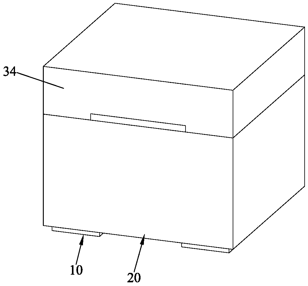
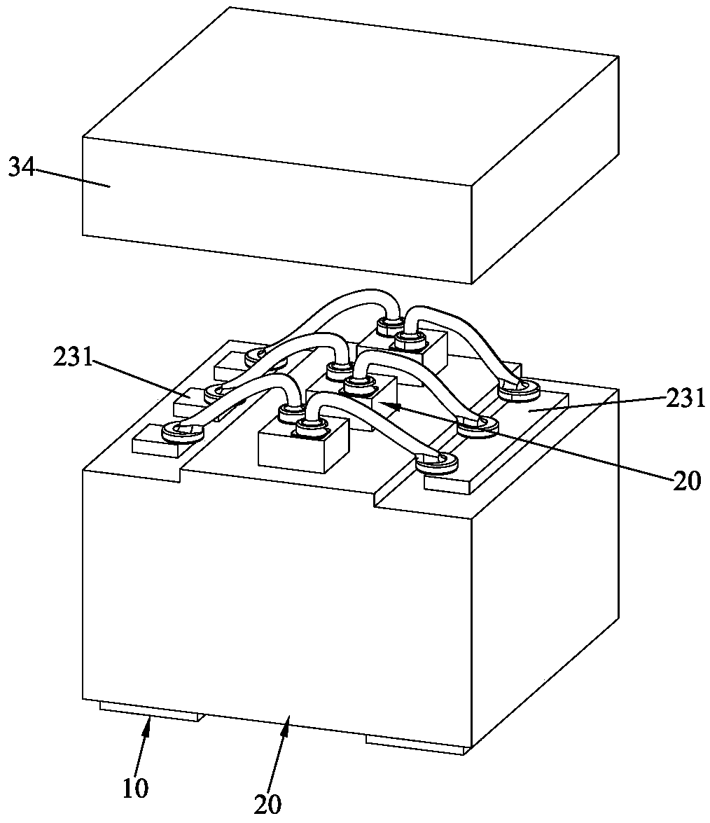
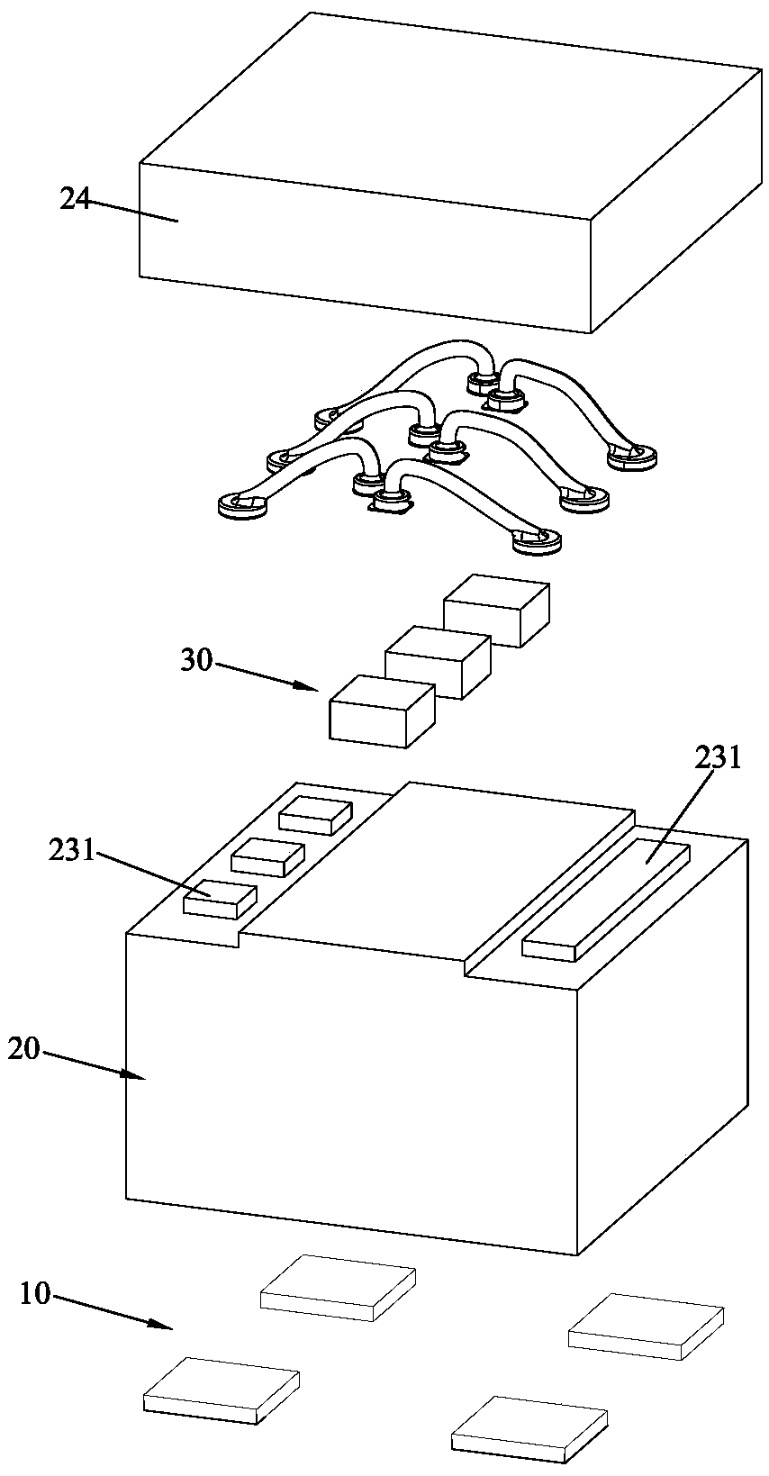
[0050] Please refer to Figure 1 to Figure 15 As shown, it shows the specific structure of a preferred embodiment of the present invention, which is an integrated photoelectric display unit 100, including a support wiring structure 10, a control drive chip 20 and a light emitting chip 30 arranged sequentially from bottom to top. .

[0051] (Such as Figure 5 As shown), the control drive chip 20 has a substrate layer 21, an RDL wiring layer 22 disposed on the top of the substrate layer 21, and an insulating layer 23 formed on the top of the RDL wiring layer 22, and the substrate layer 21 is preferably a silicon substrate; The upper surface of the insulating layer 23 is exposed with a number of welding positions 231, and the welding positions 231 are electrically connected to the RDL wiring layer 22; the support wiring structure 10 includes a plurality of electrodes, and the support wiring structure 10 is integrated on the substrate layer. 21 at the bottom, the electrode and t...


PUM


Abstract

The invention discloses an integrated photoelectric display unit, a manufacturing process thereof and a photoelectric display device. A bracket wiring structure, a control driving chip and a light emitting chip are comprised. The control driving chip comprises a substrate layer, an RDL wiring layer arranged on the top of the substrate layer, and an insulating layer formed on the top of the RDL wiring layer. A number of soldering sites are exposed on the upper surface of the insulating layer. The soldering sites are electrically connected with the RDL wiring layer. A substrate layer passes through the space between an electrode and the RDL wiring layer, which are connected through a silicon via technology. The light emitting chip is placed on the top of the control driving chip and connected with the corresponding soldering site. The bracket wiring structure and the light emitting chip are integrated on the control driving chip. The overall size thereof can be made smaller, and is closest to the lamp bead volume which is the pixel unit volume. According to the photoelectric display device using the integrated photoelectric display unit, the physical spacing between each two photoelectric display units can be greatly shortened. The pixel of the photoelectric display device can be improved. Higher display precision requirements can be realized.

Description

technical field [0001] The invention relates to the technology in the field of optoelectronic display, in particular to an integrated optoelectronic display unit, a manufacturing process thereof, and an optoelectronic display device. Background technique [0002] Most of the large-size display screens on the market currently have some problems, such as: 1. The drive circuit, control chip, PCB bracket, and light-emitting board are separated, manufactured separately and then connected and assembled, resulting in a large screen thickness and a large overall physical size. 2. The control circuit is complicated, the wiring takes up a lot of space, and it is difficult to improve the display accuracy of the outdoor high-brightness large-size screen; 3. The lamp beads, chips, and brackets are made separately, so that the physical distance of the pixel units is large when splicing. Higher display accuracy requirements cannot be achieved. Contents of the invention [0003] In view ...

Claims


Application Information

Patent Timeline
IPC IPC(8): H01L23/31H01L23/48H01L23/50H01L25/16G09F9/30H01L21/56H01L21/60
CPCH01L25/167H01L23/481H01L23/50H01L23/3114H01L25/50H01L24/81H01L21/56G09F9/30H01L2224/81986H01L2224/49113H01L2224/48465H01L2224/97H01L2224/48091H01L2924/00014
Inventor 刘明剑朱更生吴振雷周凯沈进辉罗仕昆
Owner DONGGUAN OPSCO OPTOELECTRONICS CO LTD
Why Eureka
Try Eureka