
Display device for displaying static pattern and manufacturing method thereof and gift box

A technology for display devices and manufacturing methods, applied in the direction of electrical components, electric solid devices, circuits, etc., can solve problems such as switching, limiting the application range of paper, and exceeding products

Inactive Publication Date: 2019-11-05
SYSKEY TECH CO LTD
View PDF4 Cites 1 Cited by
  • Summary
  • Abstract
  • Description
  • Claims
  • Application Information

AI Technical Summary

Problems solved by technology

However, for the requirement of displaying specific patterns, such as business cards or explanatory boards, although traditional display devices can display specific patterns to meet this requirement, the cost is too high, even far exceeding the original price of the product, so traditional The display device will not be applied to these requirements
At present, the demand for displaying specific patterns is generally only met by printed paper. Although the desired pattern can be displayed, the user can directly see the pattern, that is, the paper cannot be switched between different states. Therefore, the scope of application of this paper is limited, and it cannot provide users with a wider range of needs.

Method used


Image

  • Display device for displaying static pattern and manufacturing method thereof and gift box
  • Display device for displaying static pattern and manufacturing method thereof and gift box
  • Display device for displaying static pattern and manufacturing method thereof and gift box

Examples


Embodiment Construction

[0034] The following will clearly and completely describe the technical solutions in the embodiments of the present invention with reference to the accompanying drawings in the embodiments of the present invention. Obviously, the described embodiments are only some, not all, embodiments of the present invention. Based on the embodiments of the present invention, all other embodiments obtained by persons of ordinary skill in the art without making creative efforts belong to the protection scope of the present invention.

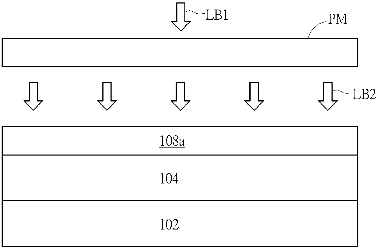
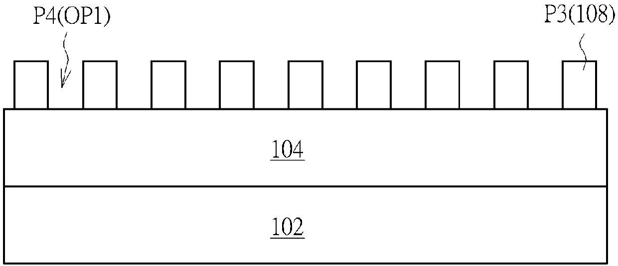
[0035] Figure 1 to Figure 7 A schematic diagram showing a manufacturing method of a display device according to a first embodiment of the present invention, wherein Image 6 is a schematic cross-sectional view of the display device according to the first embodiment of the present invention, Figure 7 It is a schematic top view of the display device according to the first embodiment of the present invention. The display device 100 of the present invention is ...


PUM

PropertyMeasurementUnit
Thicknessaaaaaaaaaa
Thicknessaaaaaaaaaa

Abstract

The invention provides a display device for displaying a first pattern, a manufacturing method of the display device and a gift box applying the display device. The display device comprises a substrate and a light emitting diode arranged on the substrate. The light emitting diode comprises a first electrode, a transparent insulating pattern layer, a light emitting layer and a second electrode. Thetransparent insulating pattern layer is arranged on the first electrode, the thickness of the transparent insulating pattern layer is smaller than or equal to 100 nanometers, and the transparent insulating pattern layer is provided with a second pattern which is complementary with the first pattern. The light-emitting layer covers the transparent insulating pattern layer and the first electrode,and the light-emitting layer is electrically connected with the first electrode. The second electrode is disposed on the light emitting layer. The display device can have a switchable pattern displaymode and a pattern-free mode.

Description

technical field [0001] The present invention relates to a display device for displaying static patterns, a manufacturing method thereof and a gift box, in particular to a display device capable of switching between a pattern display mode and a non-pattern mode, a manufacturing method thereof and a gift box using the display device. Background technique [0002] In order to display patterns according to requirements, a conventional display device includes an active array circuit and a plurality of pixels, and the display of the pixels is controlled by the active array circuit. However, for the requirement of displaying specific patterns, such as business cards or explanatory boards, although traditional display devices can display specific patterns to meet this requirement, the cost is too high, even far exceeding the original price of the product, so traditional The display device will not be applied to these requirements. At present, the demand for displaying specific patt...

Claims


Application Information

Patent Timeline
IPC IPC(8): H01L27/32
CPCH10K59/221
Inventor 江佳玲吴学宪赖奕廷
Owner SYSKEY TECH CO LTD
Learn More