Supercharge Your Innovation With Domain-Expert AI Agents!

Circuit board forming method

A molding method and circuit board technology, applied in the directions of printed circuit, printed circuit manufacturing, insulating substrate/layer processing, etc., can solve the problems that the waste cannot be completely removed, increase the difficulty, etc., and improve the efficiency and accuracy of subsequent automatic installation. High and efficient effect

Inactive Publication Date: 2019-11-08
苏州赛提发精密科技有限公司
View PDF4 Cites 0 Cited by
  • Summary
  • Abstract
  • Description
  • Claims
  • Application Information

AI Technical Summary

Problems solved by technology

[0002] as attached Figure 1-2 As shown, the circuit board made by the traditional method generally has a plurality of circuit board units with specific functions regularly arranged on one board; the circuit board units with specific functions need to punch installation holes and cut, currently Conventional stamping dies are usually used for punching and cutting. When the stamping die is withdrawn, the waste in the mounting hole cannot be completely removed, and there is always waste in the mounting hole, which will give a circuit board with specific functions in the future. The automatic installation of the unit on the product increases the difficulty, so the automatic installation of the circuit board unit with specific functions on the product needs to ensure that all the waste in the installation hole comes out

Method used


Image

  • Circuit board forming method
  • Circuit board forming method

Examples


no. 1 example

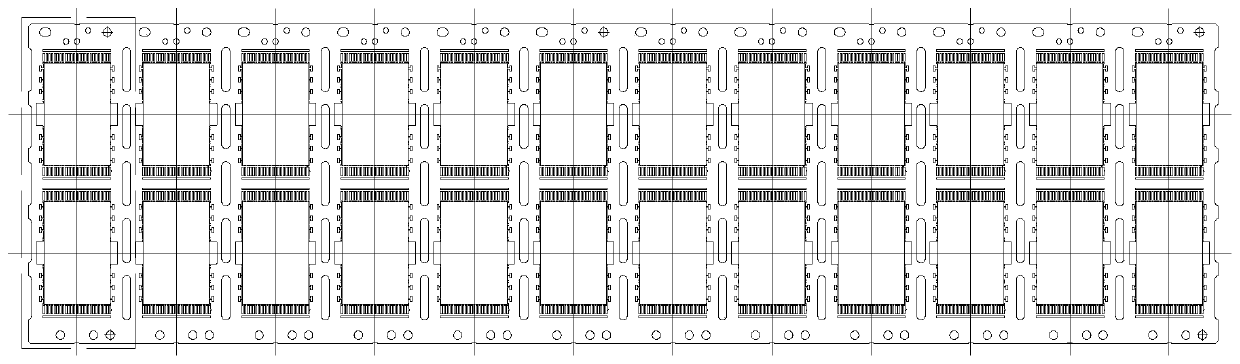
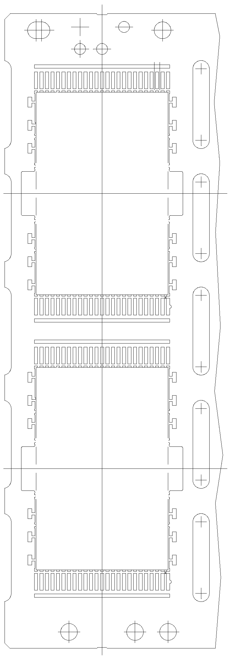
[0019] Reference Figure 1-2 , A first embodiment of a method for forming a circuit board includes the following steps:

[0020] 1. Cover the upper surface of the circuit board with an electrostatic film; the electrostatic film is made of PE material;

[0021] 2. Punching and cutting the circuit board with a stamping die according to the design requirements;

[0022] three. Tear off the electrostatic film from the cut circuit board, and at the same time take out all the waste generated by the punching;

[0023] 4. Arrange the cut circuit boards neatly and put them into the material box.

no. 2 example

[0024] Reference Figure 1-2 , A second embodiment of a method for forming a circuit board includes the following steps:

[0025] 1. Cover the lower surface of the circuit board with an electrostatic film; the electrostatic film is made of PVC;

[0026] 2. Punching and cutting the circuit board with a stamping die according to the design requirements;

[0027] three. Tear off the electrostatic film from the cut circuit board, and at the same time take out all the waste generated by the punching;

[0028] 4. Arrange the cut circuit boards neatly and put them into the material box.

[0029] Compared with the prior art, the circuit board forming method of the present invention has the following beneficial effects:

[0030] The circuit board molding method of the present invention uses the electrostatic adsorption function of the electrostatic film to take out all the waste generated by punching. The waste removal efficiency of the present invention is high, and the accuracy rate is high, wh...


PUM


Abstract

The invention discloses a circuit board forming method, which comprises the following steps: 1, the surface of the circuit board is covered with an electrostatic film; 2, the circuit board is punchedand cut by using a punching die according to design requirements; 3, the electrostatic film is removed from the cut circuit board, and all the waste generated by punching is taken out at the same time; and 4, the cut circuit boards are arranged in order to be put in a material box. The circuit board forming method disclosed in the invention uses the electrostatic adsorption function of the electrostatic film to take out all the waste generated by punching. The efficiency of removing the waste is high, the accuracy is high, and the subsequent automatic installation efficiency of the cut circuitboard is improved.

Description

Technical field [0001] The invention relates to the improvement of the manufacturing method of the circuit board, in particular to a molding method of the circuit board which uses the principle of electrostatic adsorption to quickly and cleanly remove the waste in the molding hole. Background technique [0002] As attached Figure 1-2 As shown, the circuit board manufactured according to the traditional method generally has a plurality of circuit board units with specific functions regularly arranged on a board; the circuit board units with specific functions need to be punched and cut for mounting holes. Conventional stamping dies are usually used for punching and cutting. When the stamping die is withdrawn, the waste in the mounting hole cannot be completely removed. There will always be waste remaining in the mounting hole, which will give the circuit board with specific functions in the future. The unit is automatically installed on the product, which increases the difficulty....

Claims


Application Information

Patent Timeline
IPC IPC(8): H05K3/00
CPCH05K3/005H05K3/0052H05K3/0055
Inventor 陈建
Owner 苏州赛提发精密科技有限公司
Features
  • R&D
  • Intellectual Property
  • Life Sciences
  • Materials
  • Tech Scout
  • Unparalleled Data Quality
  • Higher Quality Content
  • 60% Fewer Hallucinations
Learn More