
A kind of baking equipment of pcb board

A technology for PCB boards and baking equipment, which is applied to printed circuits, electrical components, and removal of conductive materials by chemical/electrolytic methods, can solve the problem of low baking efficiency of baking equipment

Active Publication Date: 2020-08-18
东莞市多普光电设备有限公司
View PDF3 Cites 0 Cited by
  • Summary
  • Abstract
  • Description
  • Claims
  • Application Information

AI Technical Summary

Problems solved by technology

[0003] Most of the existing baking equipment includes a conveying part and a baking part. The conveying part uses clips to clamp the edge of the PCB board (after printing, there is no photosensitive material only on the edge of tens of microns) and then cooperates with the conveyor chain through the clips, etc. Realize that the PCB passes through the baking equipment, and then complete the drying of the PCB board. However, the baking efficiency of the existing baking equipment is not high. When connecting with the printing and exposure equipment, the operating efficiency of the printing and exposure equipment needs to be reduced In order to achieve the effect of on-line operation, or need to be equipped with multiple ovens and one printing equipment to ensure processing efficiency

Method used


Image

  • A kind of baking equipment of pcb board
  • A kind of baking equipment of pcb board
  • A kind of baking equipment of pcb board

Examples


Embodiment Construction

[0024] In order to enable those skilled in the art to better understand the technical solution of the present invention, the present invention will be described in detail below in conjunction with the accompanying drawings. The description in this part is only exemplary and explanatory, and should not have any limiting effect on the protection scope of the present invention. .

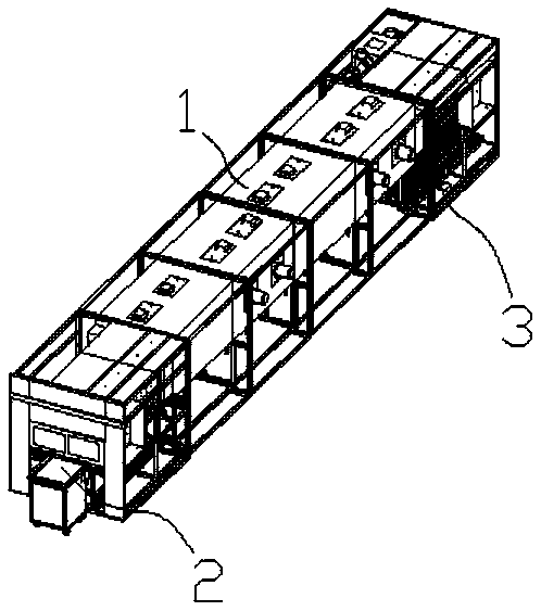
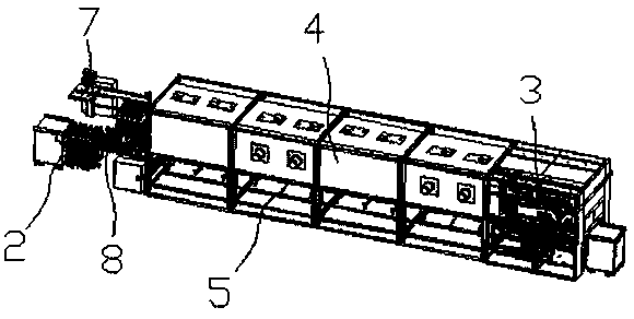
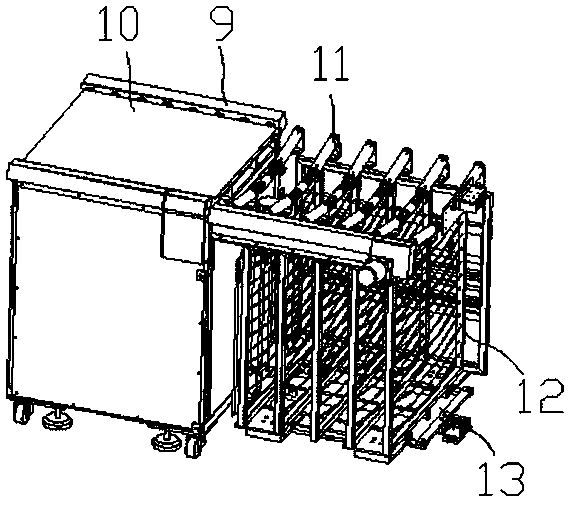
[0025] Such as Figure 1-Figure 2 As shown, the specific structure of the present invention is: a baking equipment for PCB boards, including a baking mechanism 1 and feeding mechanisms 2 and discharging mechanisms 3 on both sides thereof, the baking mechanism 1 is divided into two layers , the upper layer is a baking device 4, and the baking device 4 includes a baking conveying device and a baking part that cooperate with the charging frame 12, and the lower layer is a circular conveying device 5 that is opposite to the conveying direction of the baking conveying device. The baking conveying device co...


PUM


Abstract

The invention relates to PCB baking equipment. The baking equipment comprises a baking mechanism, and a feeding mechanism and a discharging mechanism, which are arranged at the two sides of the bakingmechanism respectively. The baking mechanism is divided into two layers, wherein the upper layer is a baking device, which comprises a baking conveying device matched with a material loading frame and a baking part; and the lower layer is a circulating conveying device opposite to the conveying direction of the baking conveying device. The baking conveying device is matched with the feeding mechanism and the discharging mechanism through feeding manipulators at the two sides; the circulating conveying device is in butt joint with the feeding mechanism and the discharging mechanism through a circulating transferring device; and the material loading frame is a frame body with at least two layers. The invention is to provide the PCB baking equipment, which adopts the multi-layer material loading frame as a carrier for PCBs moving in the baking equipment, and makes the baking equipment designed into two layers and matched with the two layers of conveying structures, so that cyclic operation of the material loading frame can be realized, the baking efficiency is improved, the baking equipment can be matched with printing equipment and exposure equipment to finish line connection, and operation efficiency of the printing and exposure equipment is not reduced.

Description

technical field [0001] The invention relates to the field of PCB board processing equipment, in particular to a PCB board baking equipment. Background technique [0002] In the process of processing the yellow light of the PCB board, the surface needs to be cleaned through the horizontal line first, and then the photosensitive material is put on the printing equipment, and then the photosensitive material needs to be pre-dried by the baking equipment (oven), and then sent to the exposure machine Expose in the middle, and finally wash through the horizontal line, so as to complete the whole process of image transfer. [0003] Most of the existing baking equipment includes a conveying part and a baking part. The conveying part uses clips to clamp the edge of the PCB board (after printing, there is no photosensitive material only on the edge of tens of microns) and then cooperates with the conveyor chain through the clips, etc. Realize that the PCB passes through the baking eq...

Claims


Application Information

Patent Timeline
Patent Type & Authority Patents(China)
IPC IPC(8): H05K3/06G03F7/38
CPCG03F7/38H05K3/06H05K2203/1105
Inventor 邱田生郭家宝李诚陈振才
Owner 东莞市多普光电设备有限公司
Learn More