A FPGA high-speed transceiver and its dynamic control method
A dynamic control, transceiver technology, applied in the direction of instruments, electrical digital data processing, etc., can solve the problem of unknown input data rate range, unable to correctly restore data and other problems, achieve simple peripheral control circuit, ensure stability, and easy to implement Effect
- Summary
- Abstract
- Description
- Claims
- Application Information
AI Technical Summary
Problems solved by technology
Method used
Image
Examples
Embodiment 1
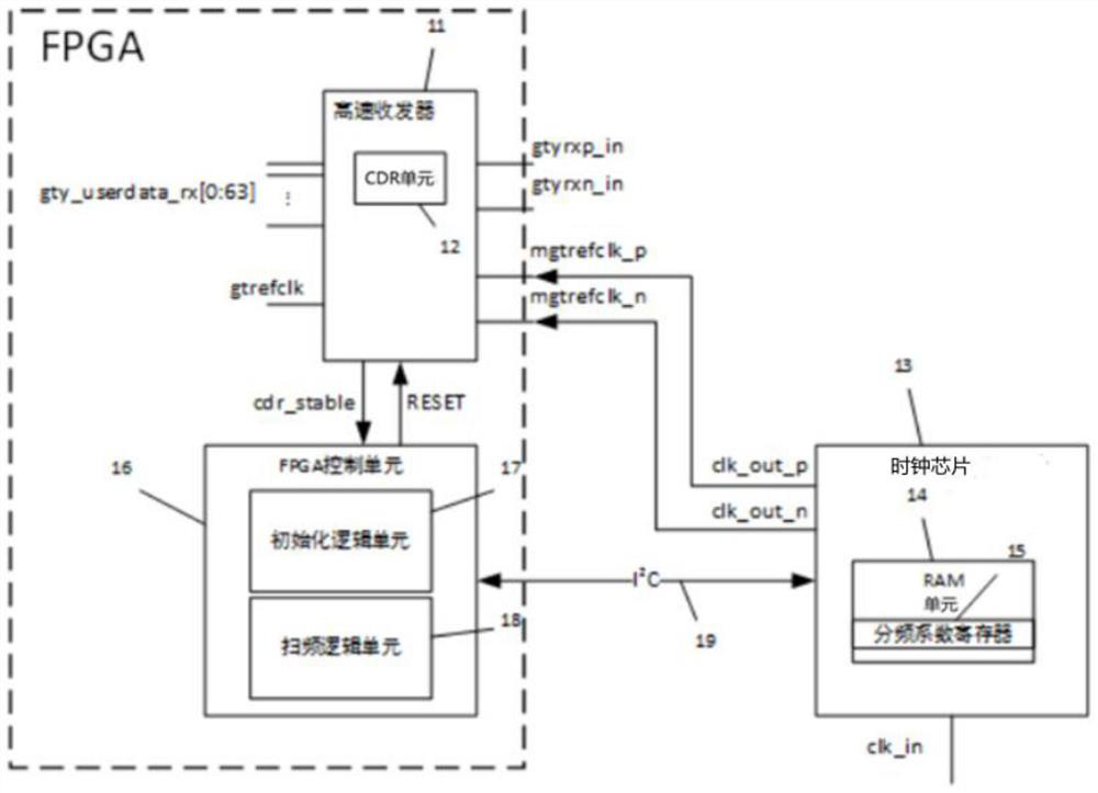
[0046] as attached figure 1 Shown a kind of FPGA high-speed transceiver, comprises the high-speed transceiver 11 of mutual connection and communication, clock chip 13, FPGA control unit 16 and I 2 C interface unit 19.
[0047] The high-speed transceiver 11 is used to provide a high-speed serial data interface, including a CDR unit 12 for completing data transmission without an associated clock; also includes a reference clock: mgtrefclk_p, mgtrefclk_n, data input: gtyrxp_in, gtyrxn_in, 64 channels of data output: gty_userdata_rx[0:63], data output clock: gtrefclk, control pin: RESET and CDR unit lock indication pin: cdr_stable; the data rate of the high-speed transceiver 11 is not less than 32Gbit / s, and the interface type It is LVDS, the driving voltage is 1.8V, the frequency difference tolerance between the input data and the reference clock is -200ppm~200ppm, ppm means one millionth, and the reference clock is ±6.55M.
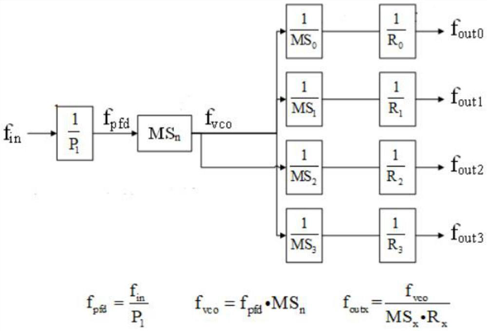
[0048] The clock chip 13 is used to divide the input...
Embodiment 2
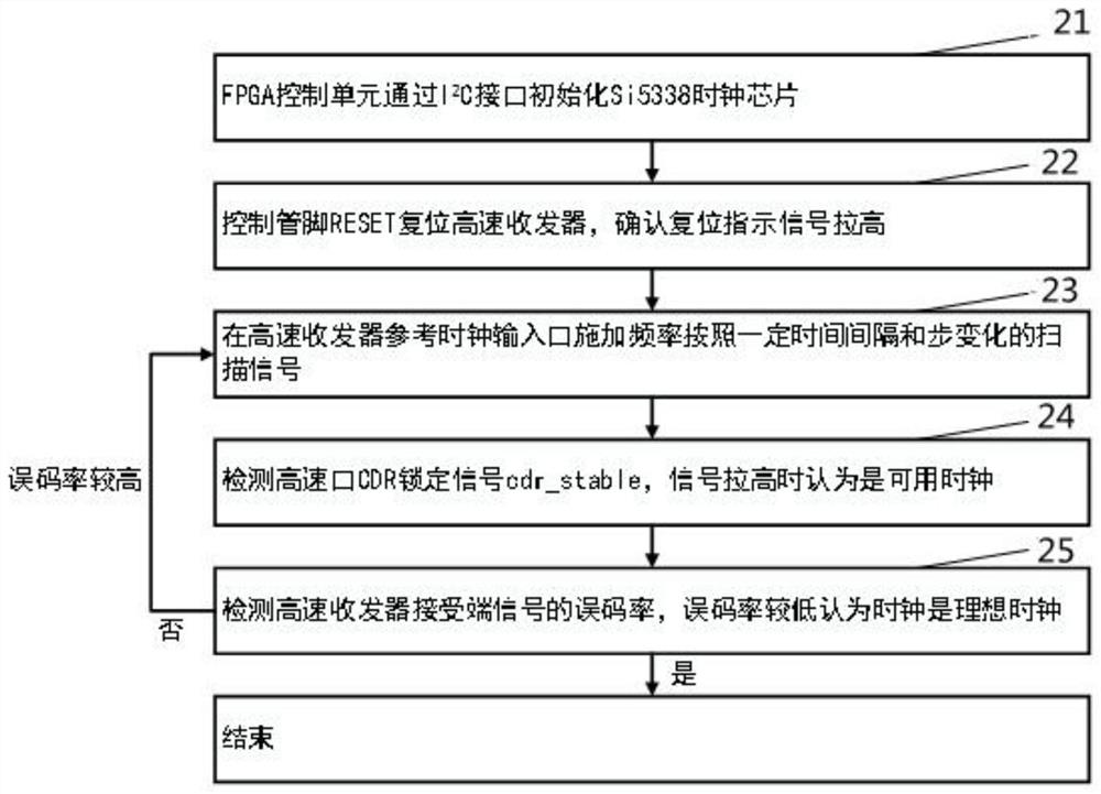
[0059] as attached image 3 The dynamic control method of a kind of FPGA high-speed transceiver shown, comprises the following steps:
[0060] Step 21, the FPGA control unit 16 passes through the I 2 The C interface unit 19 writes the initialization program of the clock chip 13 into the RAM unit 14; 350 programs are written into the frequency division coefficient register 15 during initialization, and the clock chip is preliminarily set 13 input and output formats, frequency division coefficients and function settings, etc., the initial clock frequency provided to the high-speed transceiver 11 is set to be 100M, the type is LVDS, and the driving voltage is 1.8V;
[0061] Step 22, the control pin RESET performs reset processing on the high-speed transceiver 11, and confirms that each reset indication signal is pulled high, so as to ensure that the subsequent clock data recovery circuit works normally;
[0062] Step 23, the FPGA control unit 16 applies a scan signal whose freq...
PUM
 Abstract
Description
Claims
Application Information


