Grouping test device for NAND Flash error rates
A test device and error rate technology, applied in the computer field, can solve the problems of uneven distribution of the erasing and writing process, low accuracy of test results, etc.
Active Publication Date: 2020-06-12
SUZHOU LANGCHAO INTELLIGENT TECH CO LTD
View PDF8 Cites 4 Cited by
- Summary
- Abstract
- Description
- Claims
- Application Information
AI Technical Summary
Problems solved by technology
[0009] The purpose of this application is to provide a grouping test device, method, equipment and readable storage medium of a NAND Flash error rate, in order to solve the uneven distribution of the erasing and writing process of the grouping test scheme of the current NAND Flash error rate, resulting in test results Problems with lower accuracy
Method used
View moreImage
Smart ImageViewing Examples

Examples
Embodiment 1
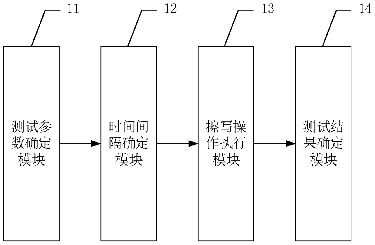
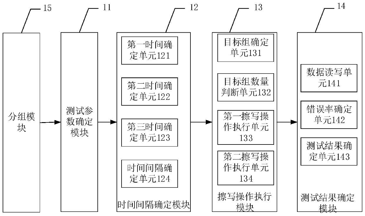
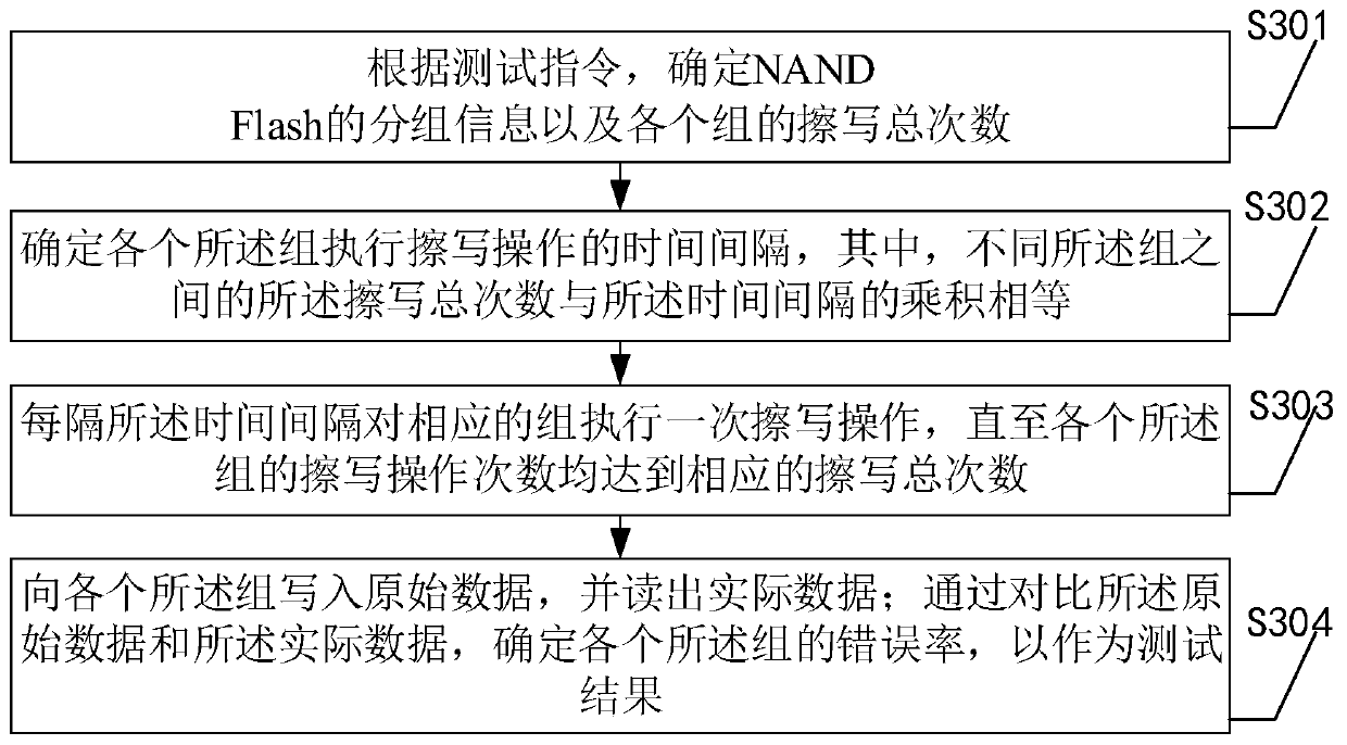
[0055] The following describes the first embodiment of a NAND Flash error rate group test device provided by this application, see figure 1 , The first embodiment includes:
Login to View More PUM
 Abstract
The invention discloses a grouping test device for NAND Flash error rates. It is guaranteed that the products of the total erasing times and time intervals of different groups are equal from the wholeNAND Flash level, and the difference value of time points when each group finishes erasing is shortened; from the single group level, erasing operation is executed on the corresponding group every other time interval, and the difference value of erasing ending time points of different Blocks in the same group is shortened; from the single Block level, erasing operation is executed on the corresponding group every other time interval, and it is guaranteed that erasing operation is conducted on each Block at equal time intervals. Therefore, based on the three levels, the distribution uniformityof the erasing and writing process is improved, and the accuracy of error rate testing is improved. The invention further provides a grouping test method and device for the NANDFlash error rate and areadable storage medium, and the technical effect of the grouping test method and device corresponds to the technical effect of the device.
Description
Technical field [0001] This application relates to the field of computer technology, and in particular to a NAND Flash error rate grouping test device, method, equipment and readable storage medium. Background technique [0002] NAND Flash is a kind of memory suitable for a large amount of data storage, composed of blocks. Every time NAND Flash is erased and written, its life will be reduced. If the life of a block is reached, the data in the block will be wrong and cannot be used reliably. Therefore, the bit error rate of the block after being erased and written several times (bit error rate) is obtained. Vital. [0003] At present, NAND Flash is generally tested for attenuation through a cyclic operation. First, multiple blocks are grouped, and the total number of erasing and writing times for each group is set, and then the error rate of each group after different erasing and writing times is obtained. For example, for MLC blocks, if you want to know the error rate of 100, 300...
Claims
Login to View More Application Information
Patent Timeline
 Patent Type & Authority Applications(China)
IPC IPC(8): G11C29/56G11C16/34
CPCG11C29/56008G11C16/349
Inventor 王敏阚宏伟王彦伟
Owner SUZHOU LANGCHAO INTELLIGENT TECH CO LTD