Pixel circuit, driving method of pixel circuit and display panel

A pixel circuit and driving source technology, which is applied in the field of pixel circuits, pixel circuit driving methods and display panels, can solve problems such as afterimages and reduce the display effect of OLED display panels, so as to reduce hysteresis effects, improve display effects, and improve residual effects. shadow effect

Pending Publication Date: 2020-06-30
KUNSHAN GO VISIONOX OPTO ELECTRONICS CO LTD
View PDF9 Cites 12 Cited by
  • Summary
  • Abstract
  • Description
  • Claims
  • Application Information

AI Technical Summary

Problems solved by technology

However, when the OLED display panel switches gray-scale images, there will be afterimage phenomenon, which reduces the display effect of the OLED display panel.

Method used


Image

  • Pixel circuit, driving method of pixel circuit and display panel
  • Pixel circuit, driving method of pixel circuit and display panel
  • Pixel circuit, driving method of pixel circuit and display panel

Examples


Embodiment Construction

[0040] The present invention will be further described in detail below in conjunction with the accompanying drawings and embodiments. It should be understood that the specific embodiments described here are only used to explain the present invention, but not to limit the present invention. In addition, it should be noted that, for the convenience of description, only some structures related to the present invention are shown in the drawings but not all structures.

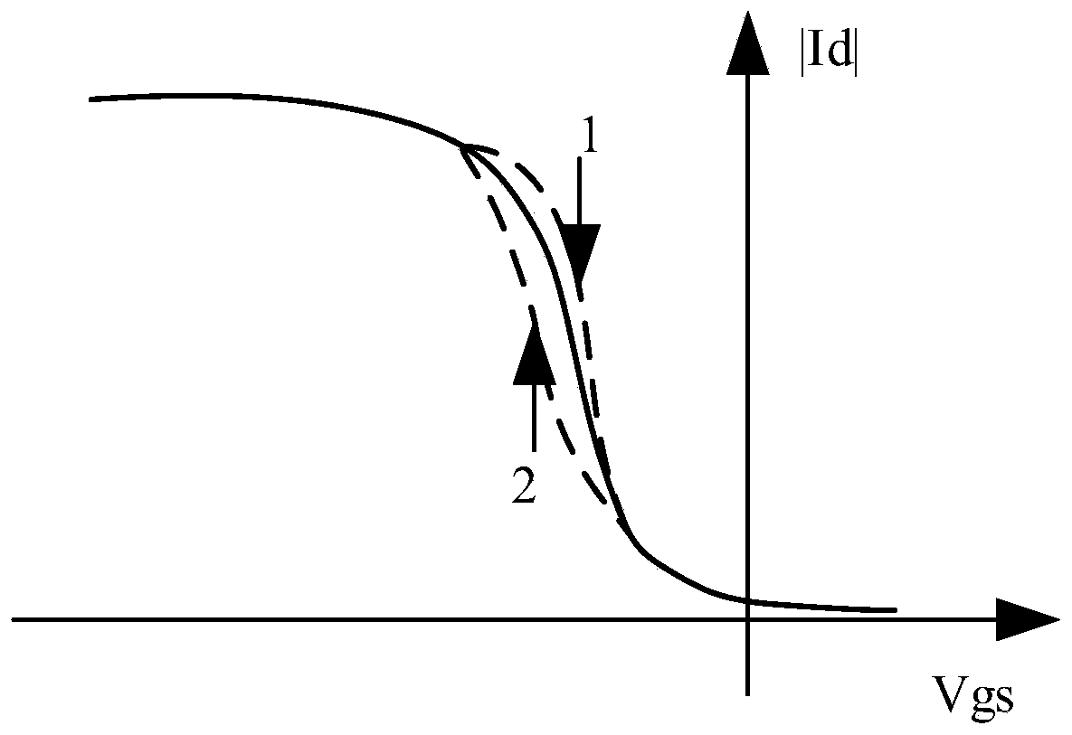
[0041] In the prior art, when the OLED display panel performs screen switching, a screen before switching does not disappear immediately, but slowly disappears with the next screen, resulting in a short-term afterimage phenomenon on the OLED display panel. For example, the OLED display panel displays a black and white checkerboard picture, the pixel units corresponding to the black checkerboard picture have lower luminance, and the gate-source voltage of the driving transistor in the pixel unit corresponding to the...


PUM


Abstract

The invention discloses a pixel circuit and a display panel. The pixel circuit comprises a driving transistor used for providing a driving current for a light-emitting device in a light-emitting stage, and the light-emitting device responds to the driving current to emit light. A first initialization module is connected between a grid electrode of the driving transistor and a first initializationpower supply end, and the first initialization module is used for providing the voltage of the first initialization power supply end to the grid electrode of the driving transistor in a first initialization stage. A second initialization module is connected between the grid electrode of the driving transistor and the second initialization power supply end, and before the first initialization stage, the voltage of the second initialization power supply end is provided for the grid electrode of the driving transistor, and the voltage of the first initialization power supply end is smaller than that of the second initialization power supply end. According to the invention, the hysteresis effect of the driving transistor can be weakened, the ghost phenomenon of the display panel where the pixel circuit is located can be further improved, and the display effect of the display panel is improved.

Description

technical field [0001] Embodiments of the present invention relate to the field of display technology, and in particular, to a pixel circuit, a driving method for the pixel circuit, and a display panel. Background technique [0002] Organic Light Emitting Diode (OLED) display panels have the advantages of low energy consumption, low production cost, self-illumination, wide viewing angle and fast response speed, and are widely used in the display field. On the other hand, when the OLED display panel switches gray-scale images, afterimage phenomenon will occur, which reduces the display effect of the OLED display panel. Contents of the invention [0003] The invention provides a pixel circuit, a driving method of the pixel circuit and a display panel to improve the afterimage phenomenon of the display panel. [0004] In a first aspect, an embodiment of the present invention provides a pixel circuit, including: [0005] a driving transistor, configured to provide a driving ...

Claims


Application Information

Patent Timeline
Patent Type & Authority Applications(China)
IPC IPC(8): G09G3/3233
CPCG09G3/3233
Inventor 胡思明齐栋宇赵欣许骥王鹏
Owner KUNSHAN GO VISIONOX OPTO ELECTRONICS CO LTD
Why Eureka
Try Eureka