Purification of carbon nanotubes via selective heating

a carbon nanotube and selective heating technology, applied in the field of carbon nanotube materials, can solve the problems of increasing static power consumption, reducing the on/off ratio of devices, affecting the commercialization of these systems, etc., and achieves the effects of low operational voltage, convenient direct comparison, and easy removal

Active Publication Date: 2016-05-12
THE BOARD OF TRUSTEES OF THE UNIV OF ILLINOIS +2
View PDF3 Cites 38 Cited by
  • Summary
  • Abstract
  • Description
  • Claims
  • Application Information

AI Technical Summary

Benefits of technology

[0119]FIG. 72. The effectiveness of the microwave-based purification process. (a) Schematic illustration of various steps to verify the effectiveness of the purification process. Fabrication and measurements of transistors built on small arrays of SWNTs (number of SWNTs from 10 to 25) before and after the purification facilitates the direct comparisons. The source and drain of the transistor also serve as the antenna for the purification. The PMMA dielectrics make the top-gate easily remove by acetone after the characterizations. Patterning new Ohmic contacts by Pd afterwards, and depositing SU8(20 nm) / HfO2(5 nm) as new dielectric lead to transistors with low operational voltage and low hysteresis. (b)(c) Typical transfer curve and output characteristics (near the on state region) for a transistor before and after the purification. The on-off ratio increases from ˜3 to ˜8.5×10⁴, and the maximum output current retains ˜40% after the purification. (d) The maximum output current before and after (Imax_b and Imax_a, respectively) purification, as a function of the ratio (Na / Nb) of the number of SWNTs after purification respect to the one before purification. Imax_b / Imax_a ranges from 0.1 to 0.6, increasing with the rise of Na / Nb, which suggests that the s-SWNTs are well protected. (e) Statistics of the on-off ratios of the transistors based on the SWNTs, before (black square) and after (red dot) the purification, respectively. The Ion / Ioff increases from <10 to 1×10³˜106, agreeing with the removal of all the m-SWNTs. (f) (g) Typical transfer curve and output characteristics of a transistor built on a small array of purified SWNTs (15 SWNTs), by using Pd as new contacts and SU8(50 nm) / HfO2(5 nm) as dielectrics. The low hysteresis feature facilitates the extraction of the device mobility, which is ˜1600 cm2 / WS as shown in the insert graph.

Problems solved by technology

Despite substantial progress in developing a SWNT-based electronic device platform, several factors impede commercialization of these systems.
Such metallic conductive pathways decrease the device on / off ratio attainable and generally increase the static power consumption, thereby preventing their applications for important classes of electronics systems.

Method used


Image

  • Purification of carbon nanotubes via selective heating
  • Purification of carbon nanotubes via selective heating
  • Purification of carbon nanotubes via selective heating

Examples


example 1

Using Nanoscale Thermocapillary Flows to Create Purely Semiconducting Arrays of Single Walled Carbon Nanotubes

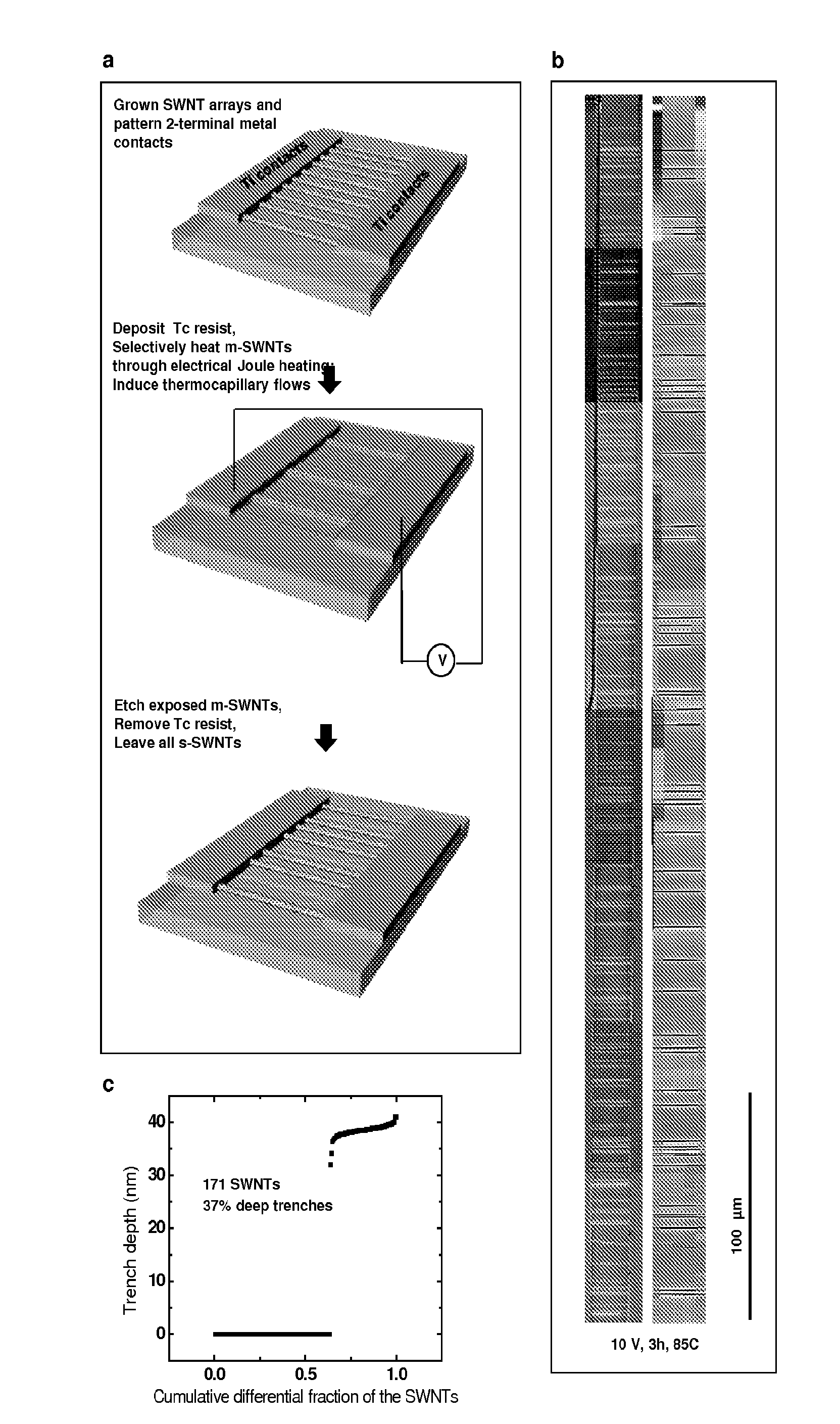
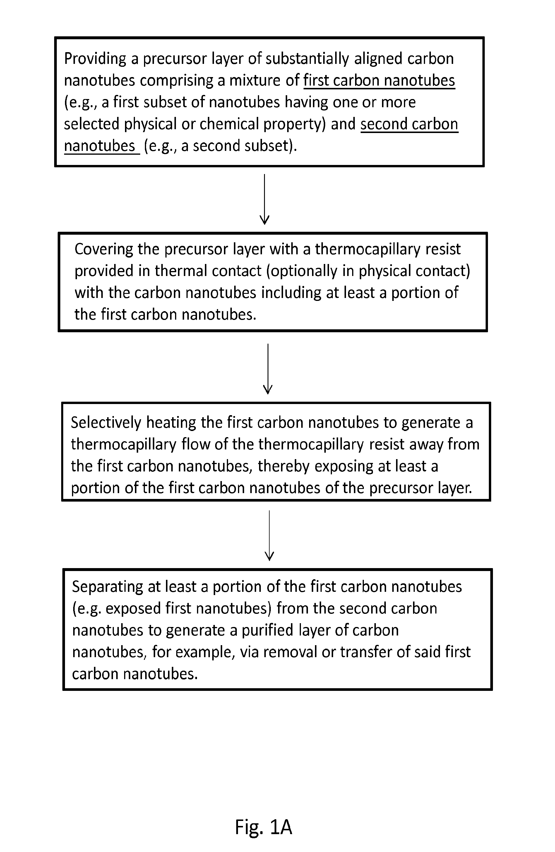
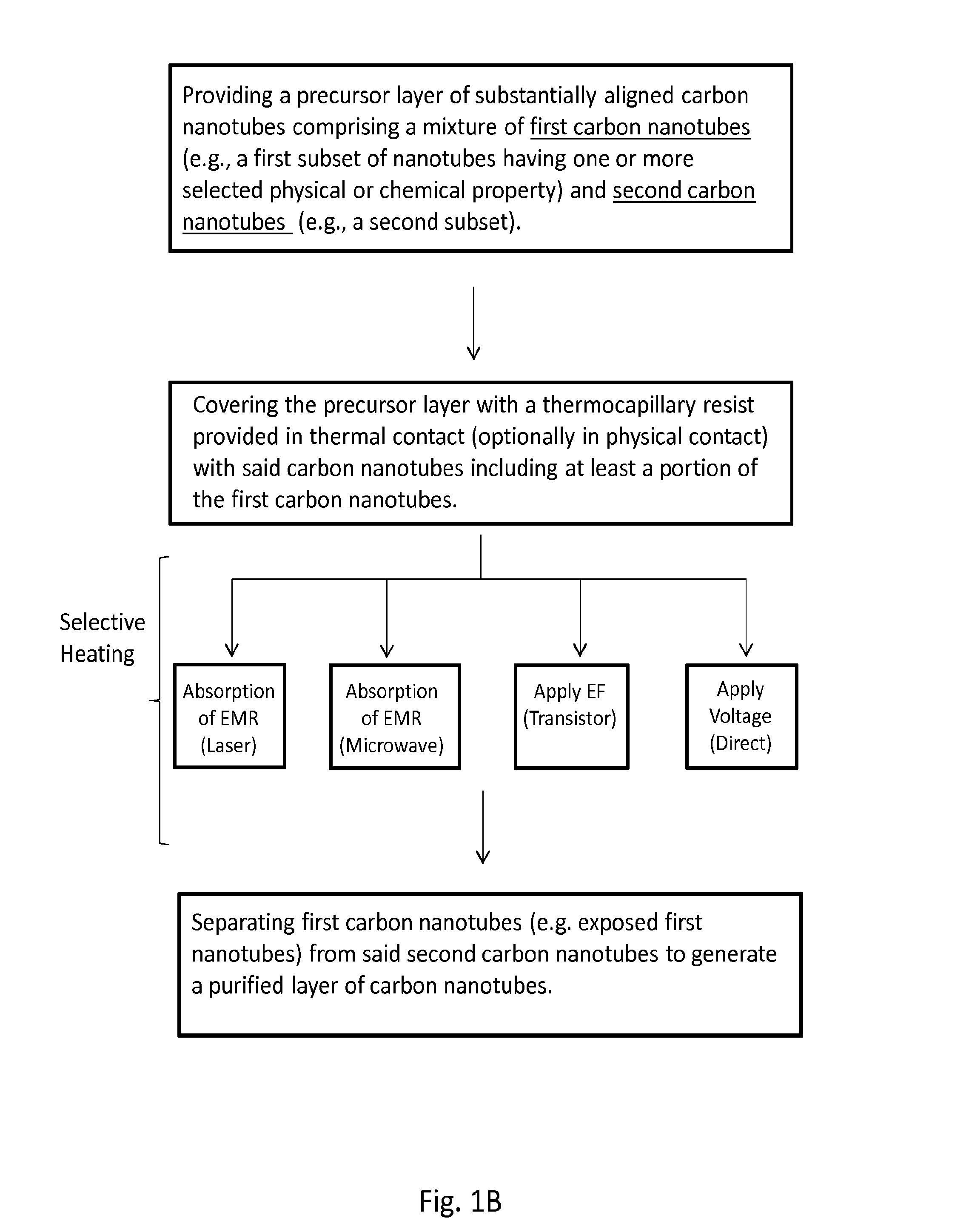
[0166]Among the remarkable variety of semiconducting nanomaterials that have been discovered over the past two decades, single walled carbon nanotubes (SWNTs) remain uniquely well suited for applications in high performance electronics, sensors and other technologies. The most advanced opportunities demand the ability to form perfectly aligned, horizontal arrays of purely semiconducting, chemically pristine SWNTs. Here, we present strategies that provide this capability, in which nanoscale thermocapillary flows in thin film organic coatings serve as highly efficient means for selectively removing metallic SWNTs from electronically heterogeneous aligned arrays grown on quartz substrates. The low temperatures and unusual physics associated with this process enable robust, scalable operation, with clear potential for practical use. Detailed experimental and theoretical studies ...

example 2

[0347]Aligned single walled carbon nanotubes (SWNTs) are well suited for applications in high dynamic range RF electronics, low-noise linear amplifiers, mixed-signal devices and sensors. During CVD growth of aligned tube arrays both metallic and semiconducting tubes naturally grow at a statistical ratio of 1:3. Many electronic device applications require arrays of purely semiconducting SWNTs. The presence of metallic nanotubes degrades the device electronic properties, impeding high performance. In the example above, we introduced nanoscale thermocapillary flow (NTF) processing in thermal resists for complete, selective removal of metallic SWNTs from CVD arrays. Here, we explore three distinct purification paths with a focus on complete process development, modeling and scalability. Microwave initiated NTF, laser initiated NTF, and direct laser ablation were assessed in detail. We have shown while all the techniques offer promise, microwave excitation is the most promising and can p...

example 3

Laser IR Based Approaches to Induce Thermocapillary Flow

[0381]A schematic of the IR-based TcEP process is presented in FIG. 68. SWNTs were grown via CVD on ST-cut quartz. A 25 nm amorphous film of α,α,α′-Tris(4-hydroxyphenyl)-1-ethyl-4-isopropylbenzene, a small organic molecule, is deposited onto the substrate. This material, hereinafter referred to as the thermocapillary(Tc) resist, was chosen for its thermal properties, resistance to RIE, as well as its ability to form a uniform and continuous ultrathin film on SWNTs and quartz. In addition, the detailed mechanisms behind thermocapillary flow of this material have been thoroughly explored in previous publications. Background heating of 65° C. was uniformly applied to the substrate, decreasing the viscosity of the Tc resist and promoting thermocapillary flow. The SWNTs were exposed using a λ=2500 nm pulsed infrared laser with a pulse duration of 10 ns and repetition rate of 1 kHz focused to a 5 μm beam spot size. The beam was raste...


PUM

PropertyMeasurementUnit
lengthaaaaaaaaaa
thicknessaaaaaaaaaa
frequencyaaaaaaaaaa

Abstract

The present invention provides methods for purifying a layer of carbon nanotubes comprising providing a precursor layer of substantially aligned carbon nanotubes supported by a substrate, wherein the precursor layer comprises a mixture of first carbon nanotubes and second carbon nanotubes; selectively heating the first carbon nanotubes; and separating the first carbon nanotubes from the second carbon nanotubes, thereby generating a purified layer of carbon nanotubes. Devices benefiting from enhanced electrical properties enabled by the purified layer of carbon nanotubes are also described.

Description

CROSS-REFERENCE TO RELATED APPLICATIONS[0001]This application claims the benefit of priority to U.S. provisional Patent Application 61 / 808,572 filed Apr. 4, 2013, which is hereby incorporated by reference in its entirety.STATEMENT REGARDING FEDERALLY SPONSORED RESEARCH OR DEVELOPMENT[0002]This invention was made with government support awarded by the following agency: U.S. Department of Energy Grant DEFG02-91 ER45439. The United States government has certain rights in the invention.BACKGROUND OF INVENTION[0003]Since their discovery in the early 1990s, a great deal has been learned about the composition and properties of carbon nanotube materials. This research has demonstrated that carbon nanotubes exhibit extraordinary mechanical, electronic and chemical properties, which has stimulated substantial interest in developing applied technologies exploiting these properties. Accordingly, substantial research is directed at developing techniques for organizing, arranging and incorporatin...

Claims


Application Information

Patent Timeline
Patent Type & Authority Applications(United States)
IPC IPC(8): H01L51/00C01B31/02
CPCH01L51/0048C01B31/026C01B2202/22C01B2202/34H01L51/0004C01B32/17Y02E60/10H10K71/311H10K85/221H01L21/02606H10K71/13B82Y30/00G01N21/62H01M4/1393
Inventor ROGERS, JOHN A.WILSON, WILLIAM L.JIN, SUNG HUNDUNHAM, SIMON N.XIE, XUISLAM, AHMEDDU, FRANKHUANG, YONGGANGSONG, JIZHOU
Owner THE BOARD OF TRUSTEES OF THE UNIV OF ILLINOIS
Why Eureka
Try Eureka