Supercharge Your Innovation With Domain-Expert AI Agents!

Display substrate and display device

A display substrate and display device technology, applied to semiconductor devices, electrical components, circuits, etc., can solve the problem of increasing the frame of the display panel

Active Publication Date: 2020-09-11
BOE TECH GRP CO LTD
View PDF16 Cites 6 Cited by
  • Summary
  • Abstract
  • Description
  • Claims
  • Application Information

AI Technical Summary

Problems solved by technology

[0003] Since there are generally only two metal layers in the display area, the gate, the source, and the drain, the fan-out wiring must use these two metal layers. Therefore, the fan-out wiring of the current special-shaped display panel can only be arranged around the display panel. area, increasing the border of the display panel
[0004] And because the large-size high-resolution display panel needs to set more fan-out lines, the frame of the display panel is further increased

Method used


Image

  • Display substrate and display device
  • Display substrate and display device
  • Display substrate and display device

Examples


Embodiment 1

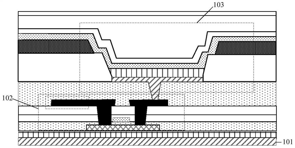
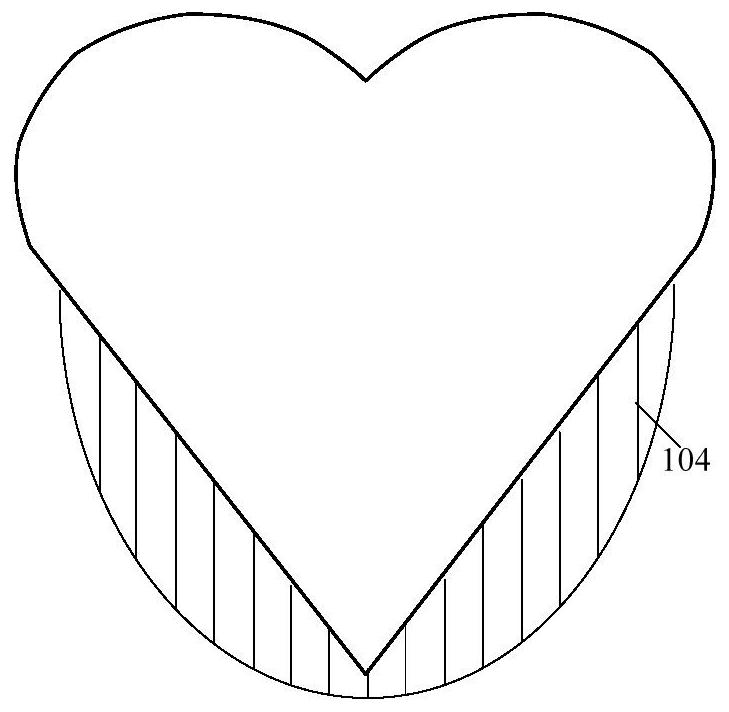
[0033] Figure 4 A schematic cross-sectional structure diagram of a display substrate provided by an embodiment of the present invention, as shown in Figure 4 As shown, the display substrate has a display area, and the display substrate includes: a substrate 101, a plurality of gate lines (not shown in the figure) located on the substrate 101, a plurality of data lines (the data lines are integrated with the source electrodes of the thin film transistors) structure, wherein the dotted line circled part of the source electrode is used as a data line); the gate line and the data line are intersected, and pixel units are defined at the intersecting positions; each pixel unit includes a thin film transistor 102 and a light emitting device located in the display area 103: The display substrate further includes a plurality of fan-out lines 104 located in the display area; wherein, the fan-out lines 104 are electrically connected to corresponding data lines, and are located in diffe...

Embodiment 2

[0050] An embodiment of the present invention provides a display device, which includes the display substrate provided in the above embodiments, and the display device may be a terminal device such as a mobile phone, a tablet computer, and a smart TV with a special shape. Its implementation principle is the same as that of the display substrate provided in the above-mentioned embodiments, and will not be repeated here.

[0051] In some embodiments, the display device further includes a driver chip; the driver chip is located on the side of the substrate 101 away from the pixel unit, and is connected to the fan-out wiring 104 in the bonding area.

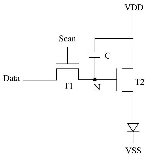
[0052] It should be noted that the driver chip can be bound and connected with the fan-out wiring 104, and provide data signals for the light-emitting devices in the pixel units through the fan-out wiring 104 and the data lines, so as to control the brightness of the light-emitting devices in each pixel unit in the display area , so ...


PUM

PropertyMeasurementUnit
thicknessaaaaaaaaaa

Abstract

The invention provides a display substrate and a display device, and belongs to the technical field of display. The technical problem that a fan-out wire in the prior art needs to be arranged in a peripheral area and needs to occupy a large frame is solved. The display substrate is provided with a display area and comprises a base, a plurality of grid lines and a plurality of data lines; and the grid lines and the data lines are located on the base. The grid lines and the data lines are arranged in a crossed mode, and pixel units are defined at the crossed positions. Each pixel unit comprisesa thin film transistor and a light-emitting device which are positioned in the display area. The display substrate further comprises a plurality of fan-out wires located in the display area, wherein the fan-out wires are electrically connected with the data lines corresponding to the fan-out wires, and the fan-out wires, the data lines and the grid lines are located in different layers.

Description

technical field [0001] The invention belongs to the field of display technology, and in particular relates to a display substrate and a display device. Background technique [0002] As application scenarios become more and more complex, regular-shaped display panels can no longer meet the needs of users, so irregular-shaped display panels are becoming more and more popular among users. In the current special-shaped display panel, a layer of fan-out wiring is generally arranged on the same layer as the film layer where the source and drain of the thin film transistor are located in the display area, and the fan-out wiring is arranged on one side of the peripheral area surrounding the display area, so that the fan-out wiring occupies Displays the border of the panel. [0003] Since there are generally only two metal layers in the display area, the gate, the source, and the drain, the fan-out wiring must use these two metal layers. Therefore, the fan-out wiring of the current ...

Claims


Application Information

Patent Timeline
Patent Type & Authority Applications(China)
IPC IPC(8): H01L27/32H01L25/18
CPCH01L25/18H10K59/131
Inventor 徐攀张大成林奕呈李永谦
Owner BOE TECH GRP CO LTD
Features
  • R&D
  • Intellectual Property
  • Life Sciences
  • Materials
  • Tech Scout
  • Unparalleled Data Quality
  • Higher Quality Content
  • 60% Fewer Hallucinations
Learn More