
Pixel structure and display panel

A pixel structure and pixel technology, which is applied in the directions of printing image acquisition, identification devices, instruments, etc., can solve the problem of increasing the difficulty of pixel arrangement structure design.

Inactive Publication Date: 2020-10-23
KUNSHAN GO VISIONOX OPTO ELECTRONICS CO LTD
View PDF6 Cites 6 Cited by
  • Summary
  • Abstract
  • Description
  • Claims
  • Application Information

AI Technical Summary

Problems solved by technology

In this way, there is also a certain requirement for the light transmittance of the display panel, which further increases the difficulty in the design of the pixel arrangement structure

Method used


Image

  • Pixel structure and display panel
  • Pixel structure and display panel
  • Pixel structure and display panel

Examples


Embodiment 1

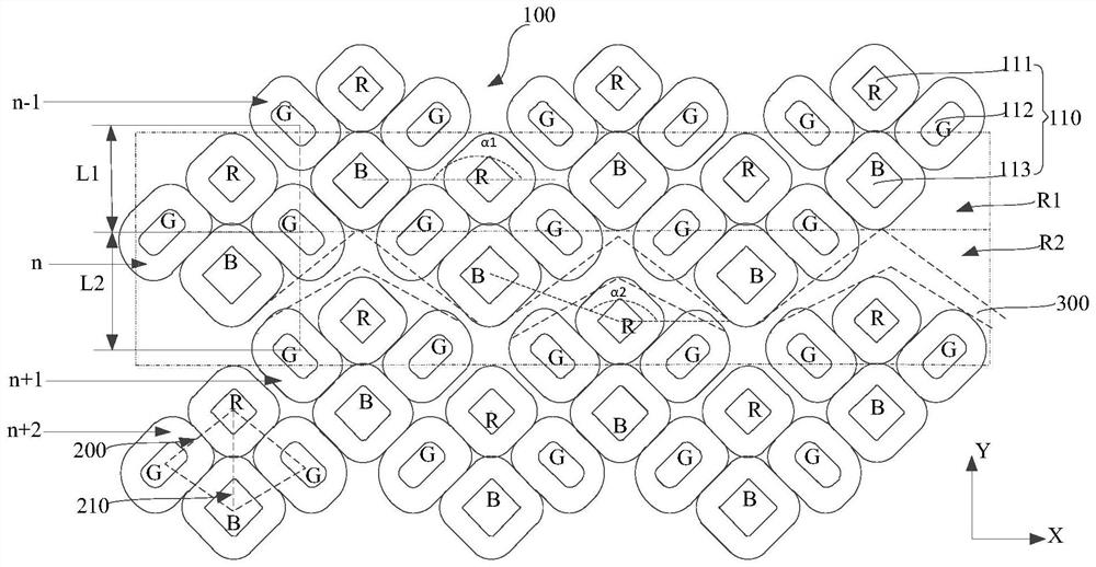
[0072] Such as figure 2 As shown, the pixel structure provided by the embodiment of the present invention includes m rows of pixel unit groups 100 (the row direction is the first direction), wherein any row can be represented by the nth row, correspondingly, along the column direction (that is, the second direction) , the row above the nth row may be called the n-1th row, and the row below the nth row may be called the n+1th row. And n is a positive integer greater than or equal to 2. Certainly, in other embodiments, the row above the nth row may also be called the n+1th row, and the row below the nth row may be called the n-1th row, and the embodiment of the present invention has no special limitation on the sequence. .

[0073] Each row of pixel unit groups 100 includes a plurality of pixel units 110 arranged at intervals along the first direction, and in any two adjacent rows of pixel unit groups 100, the pixel units 110 in one row of pixel unit groups 100 are the same a...

Embodiment 2

[0112] A second aspect of the embodiments of the present invention provides a display panel, which includes the above-described pixel structure, wherein the display panel can be applied to a tablet computer, a smart phone, and other mobile terminals or other terminal devices.

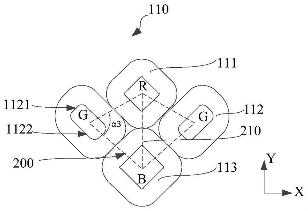
[0113] In the pixel structure provided by the embodiment of the present invention, on the one hand, each pixel unit includes a first sub-pixel, two second sub-pixels and a third sub-pixel, and the two second sub-pixels are arranged along the first direction In the same row, the first sub-pixel is located on one side of the line connecting the centers of the two second sub-pixels, and the third sub-pixel is located on the other side of the line connecting the centers of the two second sub-pixels; in this way, in each pixel unit, more The sub-pixels are not arranged on a straight line, but arranged in a two-dimensional figure (without considering the height direction), which can improve the PPI of the pixe...


PUM


Abstract

The invention provides a pixel structure and a display panel, which relate to the technical field of display. The pixel structure comprises m rows of pixel unit groups, each row of pixel unit groups comprises a plurality of pixel units, each pixel unit comprises a first sub-pixel, two second sub-pixels and a third sub-pixel, the two second sub-pixels are arranged in the same row in the first direction, and the first sub-pixel and the third sub-pixel are located on the two sides of a center connecting line of the two second sub-pixels, so that the problem that moire patterns are formed during low PPI display can be effectively solved. Furthermore, the pixel structure comprises a first layout area and a second layout area, the angles between the center connecting line of the first sub-pixeland the second sub-pixel in the two layout areas and the first direction are different, and thus, the distances between the nth row of pixel unit groups and the (n-1)th row of pixel unit groups and the (n+1)th row of pixel unit groups are different, so that a light-transmitting gap is formed between the two rows of pixel unit groups with relatively large row distances, and the light transmittanceof the pixel structure is improved.

Description

technical field [0001] The present invention relates to the field of display technology, in particular to a pixel structure and a display panel. Background technique [0002] With the continuous development of display technology, more and more photosensitive devices are installed in the display area under the screen. For example, a fingerprint identification device is installed in the display area under the screen. Wherein, the photosensitive device for fingerprint image acquisition may include an optical sensor, and the optical sensor may include a plurality of photosensitive points, which can respectively receive light signals reflected from different positions of the object, and convert the incident light into electrical signals, thereby generating image of the object. Therefore, the amount of incoming light and the contrast of the light signal received by the photosensitive point will affect the image quality of the generated object. In this way, there is also a certai...

Claims


Application Information

Patent Timeline
IPC IPC(8): G09F9/302G06K9/00
CPCG09F9/302G06V40/1318
Inventor 马天刘明星王煜侯洁白赵栋邵静
Owner KUNSHAN GO VISIONOX OPTO ELECTRONICS CO LTD
Learn More