Pixel structure, display substrate and display device
What is AI technical title?
AI technical title is built by Patsnap AI team. It summarizes the technical point description of the patent document.
A pixel structure and display substrate technology, which is applied in the field of pixel structure, display substrate and display device, can solve the problems affecting the display effect and achieve the effect of increasing the number of pixels
Active Publication Date: 2017-07-18
BOE TECH GRP CO LTD +1
View PDF10 Cites 0 Cited by
Summary
Abstract
Description
Claims
Application Information
AI Technical Summary
This helps you quickly interpret patents by identifying the three key elements:
Problems solved by technology
Method used
Benefits of technology
Problems solved by technology
When a triangle is displayed, the lit pixels are arranged as figure 2 As shown, the sum of the number of blue sub-pixels and red sub-pixels is equal to the number of green sub-pixels, between the lit pixels and non-lit pixels, red sub-pixels dominate from the upper right to the lower left, and in the display line When the display boundary is red, blue, red, and blue sub-pixels are vertically arranged alternately, or a single green sub-pixel is vertically arranged, it is visually displayed as a colored outline, which affects the display effect
Method used
Image
Click on the blue label to locate the original text in one second.
Reading with bidirectional positioning of images and text.
Examples
Embodiment 1
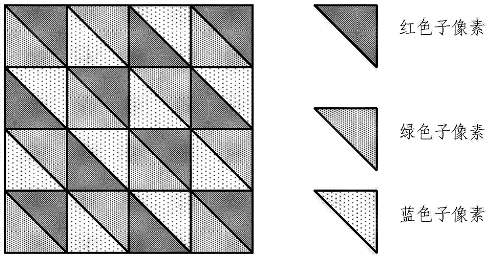
[0053] Such as image 3 and Figure 4 As shown, the pixel structure according to one embodiment of the present invention includes:
[0054] a plurality of first pixels, second pixels and third pixels,
[0055] The first pixel includes a first sub-pixel located at the upper right and a second sub-pixel located at the lower left,
[0056] The second pixel includes a second sub-pixel located at the upper right and a third sub-pixel located at the lower left,
[0057] The third pixel includes a third sub-pixel located at the upper right and a first sub-pixel located at the lower left,
[0058] The second pixel is disposed on the right and above the first pixel, the third pixel is disposed on the right and above the second pixel, and the first pixel is disposed on the right and above the third pixel.
[0059] Since each pixel includes two sub-pixels, the number of each type of sub-pixel in the pixel structure is equal, and when driven by a sub-pixel rendering method, sub-pixels...
Embodiment 2
[0073] Such as Figure 11 As shown, the pixel structure according to another embodiment of the present invention includes:
[0074] a plurality of first pixels, second pixels and third pixels,
[0075] The first pixel includes a first sub-pixel located at the upper left and a second sub-pixel located at the lower right,
[0076] The second pixel includes a third sub-pixel located at the upper left and a first sub-pixel located at the lower right,
[0077] The third pixel includes a second sub-pixel located at the upper left and a third sub-pixel located at the lower right,
[0078] The second pixel is disposed on the right and below the first pixel, the third pixel is disposed on the right and below the second pixel, and the first pixel is disposed on the right and below the third pixel.
[0079] Preferably, the first sub-pixel, the second sub-pixel and the third sub-pixel are right-angled triangles,
[0080] The first sub-pixel in the first pixel corresponds to the hypote...
PUM
Abstract
The present invention relates to a pixel structure, a display substrate, and a display device. The pixel structure includes: a plurality of first pixels, second pixels, and third pixels. The first pixel includes a first sub-pixel located at the upper right and a second sub-pixel located at the lower left. sub-pixels, the second pixel includes a second sub-pixel at the upper right and a third sub-pixel at the lower left, the third pixel includes a third sub-pixel at the upper right and a first sub-pixel at the lower left, the first pixel A second pixel is arranged on the right and above the second pixel, a third pixel is arranged on the right and above the second pixel, and a first pixel is arranged on the right and above the third pixel. Through the technical solution of the present invention, when the pixel structure displays an image with oblique boundaries, horizontal boundaries and / or vertical boundaries, the boundaries of the image are interlaced by three types of pixels: the first sub-pixel, the second sub-pixel and the third sub-pixel Arrangement, there will be no color outline phenomenon.
Description
technical field [0001] The present invention relates to the field of display technology, in particular, to a pixel structure, a display substrate and a display device. Background technique [0002] With the development of display technology, people's pursuit of visual effects is getting higher and higher, so display products with high PPI (pixels per unit area) have become the focus of attention of display manufacturers. [0003] In a traditional display substrate, the pixel structure adopts a circular arrangement of RGB (red, green, and blue) sub-pixels. Each pixel has the same area and is composed of horizontally arranged red, green, and blue sub-pixels. The area of each sub-pixel is the same. figure 1 shown. When the display substrate adopting this pixel structure displays images, the visual resolution is the same as the physical resolution. [0004] Driving the sub-pixels through the sub-pixel rendering method can achieve a visual resolution greater than the physical...
Claims
Application Information
Patent Timeline
Application Date:The date an application was filed.
Publication Date:The date a patent or application was officially published.
First Publication Date:The earliest publication date of a patent with the same application number.
Issue Date:Publication date of the patent grant document.
PCT Entry Date:The Entry date of PCT National Phase.
Estimated Expiry Date:The statutory expiry date of a patent right according to the Patent Law, and it is the longest term of protection that the patent right can achieve without the termination of the patent right due to other reasons(Term extension factor has been taken into account ).
Invalid Date:Actual expiry date is based on effective date or publication date of legal transaction data of invalid patent.

