Evaporation Donor Substrate, Method for Manufacturing the Same, and Method for Manufacturing Light-Emitting Device

a donor substrate and donor technology, applied in vacuum evaporation coating, transportation and packaging, coatings, etc., can solve the problems of increasing the number of pixels, reducing the size of a light-emitting device including, and heat absorption cannot be avoided, so as to reduce the production cost of the evaporation donor substrate, the effect of reducing the production cost and high definition

Active Publication Date: 2009-07-02
SEMICON ENERGY LAB CO LTD
View PDF33 Cites 41 Cited by
  • Summary
  • Abstract
  • Description
  • Claims
  • Application Information

AI Technical Summary

Benefits of technology

[0033]In an evaporation donor substrate of the present invention, films that are stacked to form the evaporation donor substrate have different thicknesses, so that the films are separately formed; thus, a desired pattern can be formed over the evaporation donor substrate. Accordingly, it is not necessary to perform a photolithography step that is generally required to form a pattern over an evaporation donor substrate, which results in reduction in production cost of the evaporation donor substrate.
[0034]In addition, by using the evaporation donor substrate of the present invention, the thickness of a film deposited on a deposition target substrate can be controlled by controlling the thickness of a material layer formed over the evaporation donor substrate. Therefore, the practitioner does not need to adjust the evaporation rate by using a thickness monitor, and thus the deposition process can be fully automated.
[0035]Furthermore, by using the evaporation donor substrate of the present invention, an evaporation material contained in the material layer that is formed over the evaporation donor substrate during deposition can be uniformly sublimed. Also in the case where the material layer contains a plurality of evaporation materials, a film containing the same evaporation materials in substantially the same weight ratio as the material layer can be deposited on a deposition target substrate. Accordingly, even in the case where a plurality of evaporation materials with different evaporation temperatures are used for deposition, by using the evaporation donor substrate of the present invention for the deposition, the evaporation rate of each evaporation material does not need to be controlled like co-evaporation. Therefore, without complicated control of the evaporation rate or the like, a desired layer containing different evaporation materials can be deposited easily and accurately.
[0036]Thus, in the method for manufacturing a light-emitting device of the present invention with the use of the aforementioned evaporation donor substrate, a flat and even film can be deposited and a minute pattern can be formed. Accordingly, a light-emitting device with high definition can be obtained, and further the characteristics of the light-emitting device can be improved.
[0037]Furthermore, in the method for manufacturing a light-emitting device of the present invention with the use of the aforementioned evaporation donor substrate, the use efficiency of an EL material can be increased. In addition, by using, for example, a lamp heater with high energy as a light source, deposition can be performed on a large area at a time, which results in reduction in production cost of the light-emitting device.

Problems solved by technology

Such needs are major problems in advancing miniaturization of display pixel pitches along with higher definition (an increase in the number of pixels) and reduction in size of a light-emitting device including a light-emitting element.
Therefore, even with the use of the high reflective layer, some heat absorption cannot be avoided.

Method used


Image

  • Evaporation Donor Substrate, Method for Manufacturing the Same, and Method for Manufacturing Light-Emitting Device
  • Evaporation Donor Substrate, Method for Manufacturing the Same, and Method for Manufacturing Light-Emitting Device
  • Evaporation Donor Substrate, Method for Manufacturing the Same, and Method for Manufacturing Light-Emitting Device

Examples


embodiment mode 1

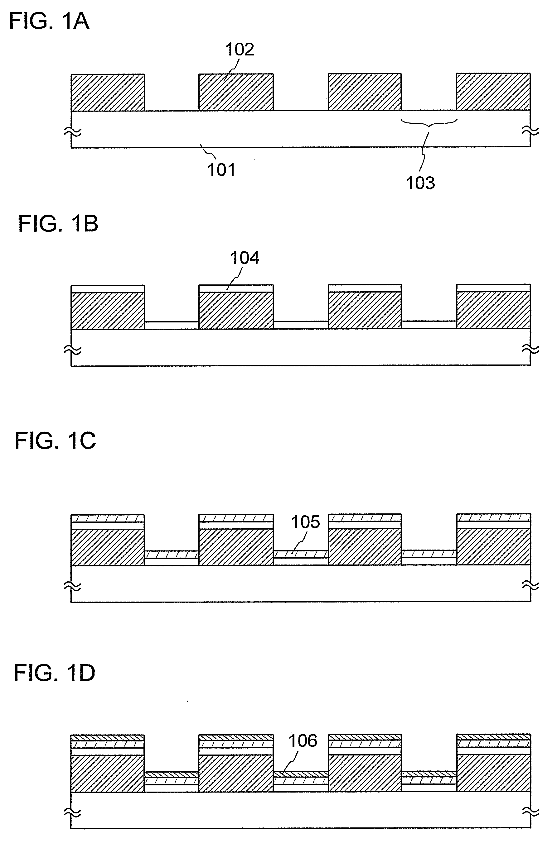
[0055]In this embodiment mode, a method for manufacturing an evaporation donor substrate in accordance with the present invention will be described.

[0056]First, as illustrated in FIG. 1A, a reflective layer 102 is formed over a first substrate 101 that is a supporting substrate. The reflective layer 102 is a layer for partially reflecting the irradiation light so that a part of a light absorption layer over an evaporation donor substrate is selectively irradiated with light during evaporation. Therefore, the reflective layer 102 is preferably formed of a material having a high reflectance for the irradiation light. Specifically, the reflective layer 102 preferably has a reflectance of 85% or more, and more preferably, a reflectance of 90% or more for the irradiation light.

[0057]As a material for the reflective layer 102, for example, silver, gold, platinum, copper, an alloy containing aluminum, or an alloy containing silver can be used. In particular, an aluminum-titanium alloy, an ...

embodiment mode 2

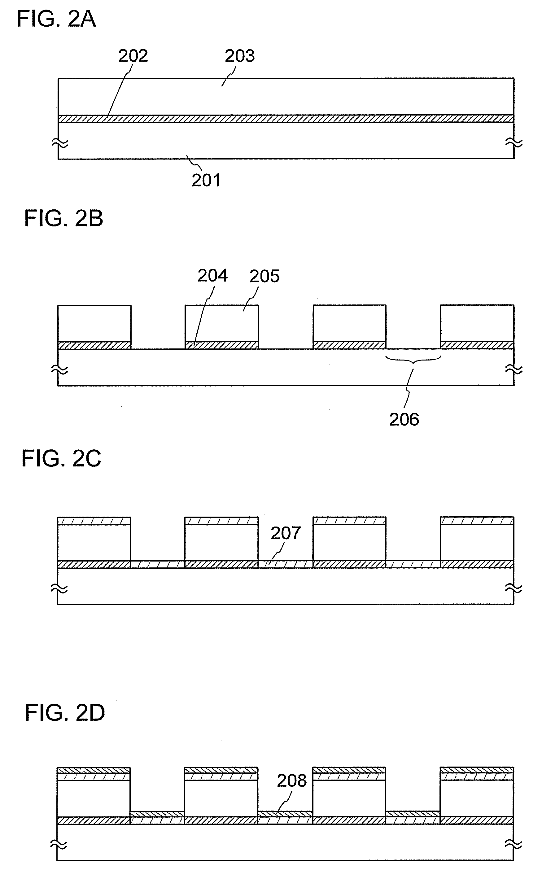
[0082]In this embodiment mode, an evaporation donor substrate having a different structure from that of the evaporation donor substrate described in Embodiment Mode 1 will be described with reference to FIGS. 2A to 2D.

[0083]First, as illustrated in FIG. 2A, a reflective layer 202 is formed over a first substrate 201 that is a supporting substrate. The reflective layer 202 is a layer for partially reflecting the irradiation light so that a part of a light absorption layer over an evaporation donor substrate is selectively irradiated with light during evaporation. Therefore, the reflective layer 202 is preferably formed of a material having a high reflectance for the irradiation light. Specifically, the reflective layer 202 preferably has a reflectance of 85% or more, and more preferably, a reflectance of 90% or more for the irradiation light.

[0084]As a material for the reflective layer 202, for example, silver, gold, platinum, copper, an alloy containing aluminum, or an alloy contain...

embodiment mode 3

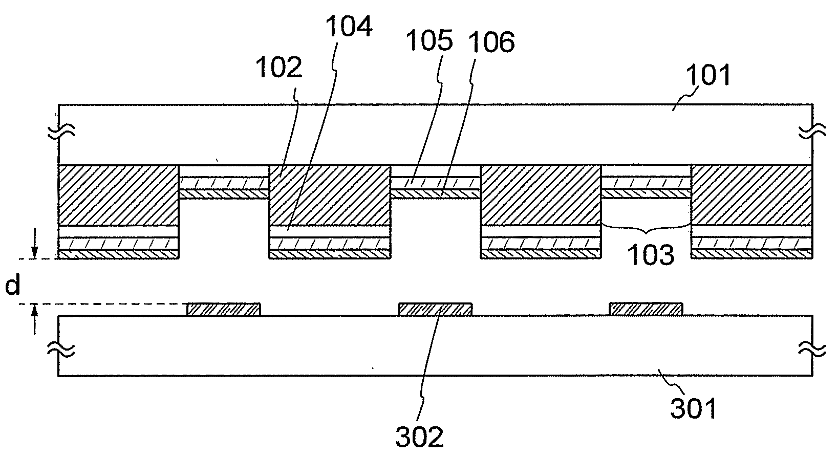
[0107]In this embodiment mode, a deposition method using an evaporation donor substrate of the present invention will be described. Note that described in this embodiment mode is a case where an EL layer of a light-emitting element is formed using the evaporation donor substrate shown in Embodiment Mode 1. The deposition method described in this embodiment mode may also be realized using the evaporation donor substrate shown in Embodiment Mode 2.

[0108]As illustrated in FIG. 3A, the reflective layer 102 is formed on the first substrate 101 that is a supporting substrate. Note that the reflective layer 102 includes the opening 103. The thermal insulation layer 104 is formed separately on the reflective layer 102 and in the opening 103 in the reflective layer 102. The light absorption layer 105 is formed on the thermal insulation layer 104.

[0109]The material layer 106 containing an evaporation material is formed on the light absorption layer 105. In FIG. 3A, due to the large thickness ...


PUM

PropertyMeasurementUnit
transmittanceaaaaaaaaaa
thicknessaaaaaaaaaa
thicknessaaaaaaaaaa

Abstract

An evaporation donor substrate that makes it possible to evaporate only a desired evaporation material in the case of performing deposition by an evaporation method. Thus, the use efficiency of an evaporation material can be increased resulting in reduction in production cost, and further a film with high uniformity can be deposited. The evaporation donor substrate can be obtained by forming a reflective layer having an opening over a substrate, forming a thermal insulation layer having a light-transmitting property separately over the substrate and the reflective layer, forming a light absorption layer over the thermal insulation layer, and forming a material layer over the light absorption layer.

Description

BACKGROUND OF THE INVENTION[0001]1. Field of the Invention[0002]The present invention relates to an evaporation donor substrate used for deposition of materials that can be deposited by an evaporation method, a method for manufacturing the evaporation donor substrate, and a method for manufacturing a light-emitting device using the evaporation donor substrate.[0003]2. Description of the Related Art[0004]Light-emitting elements using an organic compound as a light emitter, which are characterized by thinness, lightweight, fast response, and direct current low voltage driving, have been expected to be applied to next-generation flat panel displays. In particular, display devices in which light-emitting elements are arranged in matrix have been considered to be superior to conventional liquid crystal display devices in terms of a wide viewing angle and good visibility.[0005]It is considered that the light emission mechanism of a light-emitting element is as follows: when a voltage is a...

Claims


Application Information

Patent Timeline
Patent Type & Authority Applications(United States)
IPC IPC(8): B32B3/10B05D5/06
CPCY10T428/24331H01L51/0013C23C14/048H10K71/18H01L2924/01022H10K50/14H10K50/865H10K2102/351
Inventor YOKOYAMA, KOHEISATO, YOSUKEAOYAMA, TOMOYATAKAHASHI, RENA
Owner SEMICON ENERGY LAB CO LTD
Why Eureka
Try Eureka