Reconfigurable tactile sensor input device

a tactile sensor and input device technology, applied in the field of reconfigurable input devices, can solve the problems of difficult handling, increased production cost, and increased labor intensity, and achieve the effect of easy integration of tactile sensors and less production cos

Inactive Publication Date: 2009-10-27
WISETOUCH CO LTD
View PDF24 Cites 210 Cited by
  • Summary
  • Abstract
  • Description
  • Claims
  • Application Information

AI Technical Summary

Benefits of technology

[0017]An additional object of the present invention is to provide a tactile sensor which may be integrated into an existing rigid or flexible circuit board design by incorporating an electrode layer into the circuit layout.
[0024]The present invention is based on a capacitance sensor of a novel design. To be of practical value for the consumer electronics market, the input device has to be inexpensive to produce and thin in size so as to fit in small, portable electronic devices such as mobile phones. To achieve this goal, a novel design for a dielectric separation layer is used between the first and the second electrode layers. This separation layer consists of a network of structures constructed from a compressible polymer material and which form a contiguous pocket of air between the shapes, which allows the structure to compress during use. This Compressible Dielectric Structure (CDS) is then deposited between the electrode layers. As opposed to more traditional foam sheets, which even in their thinnest forms are still relatively thick, this novel approach allows the CDS, and thus the entire sensor, to be extremely thin after construction. In some embodiments, the compressible dielectric structure is made to buckle under a certain threshold pressure to provide tactile feedback to the user.
[0025]Another extension beyond traditional tactile sensors is the mounting of a sensor on a rigid substrate. While traditional tactile sensors are made flexible and sensitive to pressure from both sides, the sensor of the invention can be made sensitive only from one side, the other side being set on a rigid surface of a substrate, either by bonding a thin tactile sensor to a rigid body or by using a rigid substrate to construct one of the electrode layers. Such a construction makes the invention much more effective as an input device while still accommodating designs requiring a flexible tactile sensor. This construction also allows for easy integration of a tactile sensor into a circuit, as a standard printed circuit board can be used to form the rigid substrate and electrodes.
[0026]A further innovation is adapting a mixed-signal (analog and digital) IC to be used as a controller for reconfigurable functions of the tactile sensor-based input device. Using a mixed-signal IC capable of measuring capacitance in combination with the thin, inexpensive tactile sensor allows the creation of an novel, economically-viable input device with a wide range of novel functions (including, but not limited to, pressure measurement as a third variable in addition to traditional X,Y location information) that may be quite useful in a number of industries including consumer electronics.

Problems solved by technology

However, for small, portable electronic devices, such as mobile phones and PDAs, the human finger is too large relative to the small-sized display.
Because of this problem, many devices provide a small stylus to interact with the touch screen which takes more time to use, is difficult to handle, and is easily lost.
However, they are susceptible to environmental changes and cannot work with non-conducting objects, such as a person wearing a glove.
This class of devices does not measure contact pressure and therefore is not always able to interpret the intent of the user.
Consequently, user interaction with these devices is limited.
Individual key buttons, however, are expensive to produce using conventional discrete electrical switches.
The touch sensor, however, can be confused by multiple-point contacts and does not provide contact force information.

Method used


Image

  • Reconfigurable tactile sensor input device
  • Reconfigurable tactile sensor input device
  • Reconfigurable tactile sensor input device

Examples


first embodiment

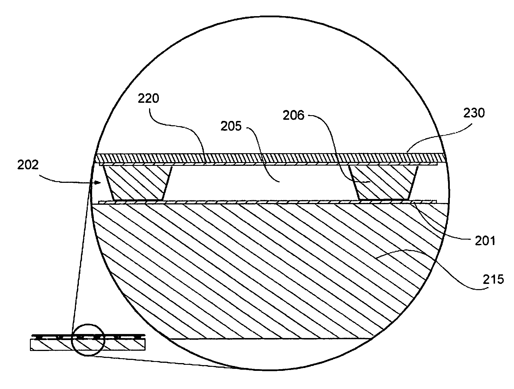
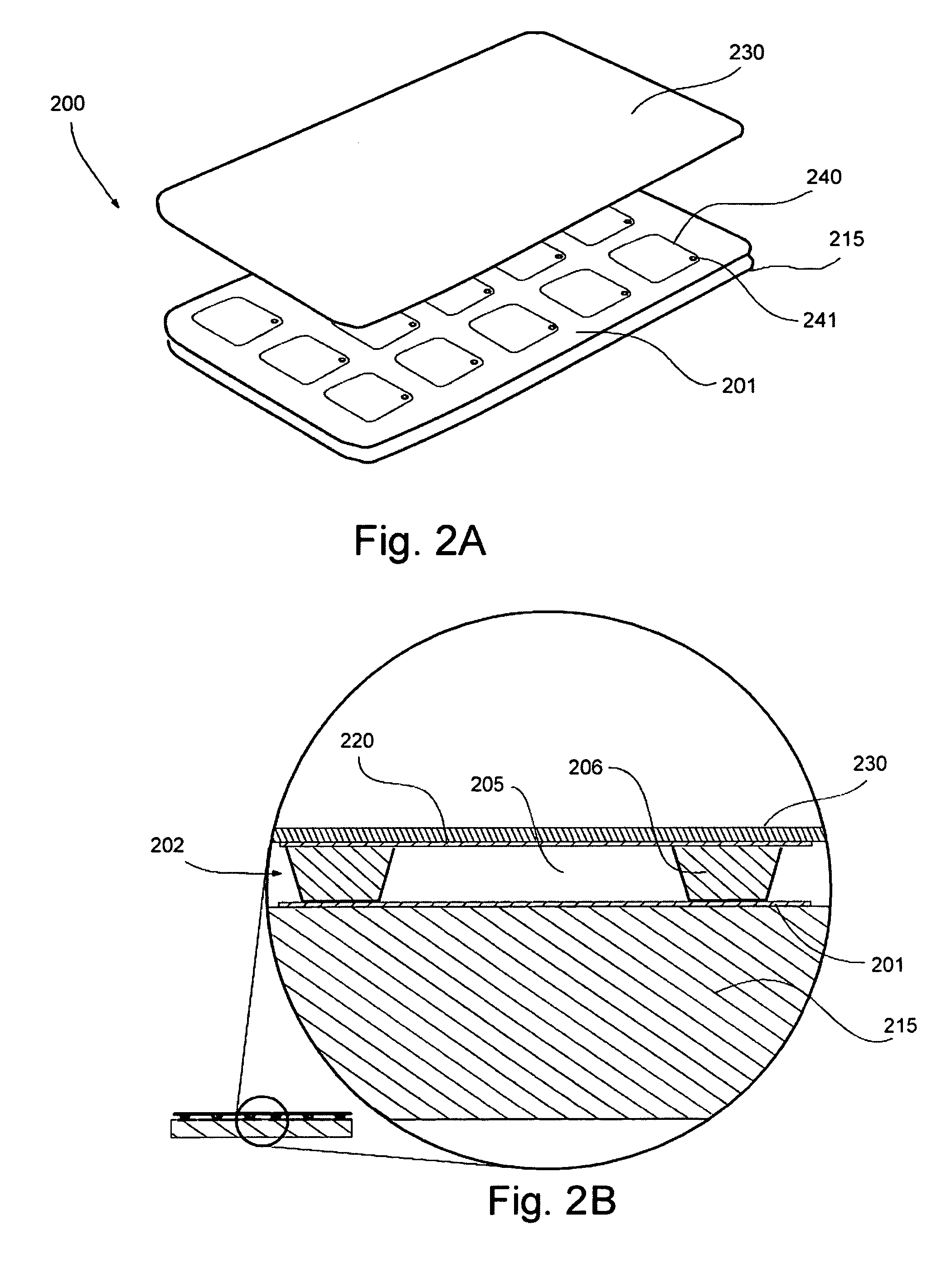
[0047]FIGS. 2A and 2B illustrate a commercially useful design of the input device 200 of the present invention. It consists of a rigid substrate 215 onto which a first layer of electrodes 201 are mounted. The electrode layer 201 can be formed using any one of a variety of standard manufacturing methods, including PCB etching, sputtered or vacuum metal deposition, or conductive ink printing methods. In this case, the first layer of electrodes is a sensing layer having discrete “button”-type electrodes 240 spaced apart throughout the sensor and supplied with electrical connection means comprising individual electrical connections (not shown) attached to the electrodes at connection points 241.

[0048]To improve electrical coupling for scrolling and other similar functions, an optional interweaving overlap between electrodes can be implemented as shown in examples on FIG. 7. FIG. 7A shows electrode design without overlap. FIGS. 7B through D show an ever increasing degree of interweaving ...

third embodiment

[0057]A full matrix of electrodes is shown as the invention on FIG. 4. Made using the same principles as the previous embodiments, this design 400 replaces discrete buttons with electrode strips 440 on the first sensing electrode layer. These strips are each equipped with an electrical connection point 441. Another set of electrode strips 421 is arranged on the second electrode layer in a direction perpendicular to the sensing electrode strips. Each upper electrode strip is also equipped with an electrical connection 422. A full electrode matrix is therefore arranged with the total number of wires needed to control the matrix being the sum of horizontal and vertical strips. In the example of the device shown on FIGS. 4, the total number of control wires is 10 for the bottom layer plus 6 for the top, totaling 16 for a 10×6 sensor array. The high spatial resolution of this matrix formed by the intersection of 421 and 440 provides for a virtually unlimited number of input device config...

fourth embodiment

[0058]the input device of the present invention is shown on FIG. 5. It has two further improvements in comparison with the previous versions: an IC 570 adapted to measure the sensor pressure values and optionally mounted nearby on the same substrate 515 as the sensor, and a flexible display means 560 overlaying the basic sensor.

[0059]The use of a commercially-available IC mounted together with the sensor allows for the mass production of the input device of the invention at an economical price. To be most useful for the purposes of the invention, the IC should be mixed-signal, allowing for both analog and digital input and output, and be capable of measuring capacitance over the entire range of electrodes, be they buttons, sliders, electrode matrices, etc. By incorporating a proprietary or standard digital interface, the IC would allow the sensor to act as a peripheral device to a host processor. This interface could take the form of any of a number of standard digital serial protoc...


PUM


Abstract

A reconfigurable tactile input device includes a first rigid electrode layer, a compressible dielectric structure, and a second flexible electrode layer forming together a tactile sensor with appropriate electrode connection means to a control means. The control means may include a mixed-signal IC mounted next to the input device in a compact package and capable of measuring capacitance in real time. The dielectric structure may include a matrix of compressible geometric elements with voids therebetween optionally vented to atmosphere, making the entire assembly thin and facilitating its use for mobile phones and other small, portable electronic devices. Some embodiments provide the user wit tactile feedback upon compression of the electrodes. An optional flexible display may be mounted over the input device to indicate the present configuration to the user.

Description

BACKGROUND OF THE INVENTION[0001]The present invention relates generally to reconfigurable input devices. More particularly, the input device of the present invention utilizes tactile sensor technology while at the same time allowing the device to change its function depending on the needs of a particular application. In one particularly advantageous embodiment, the tactile input device is capable of measuring contact location and pressure in multiple locations simultaneously to increase the error-free processing of the commands. In another embodiment, tactile feedback is provided to the user upon compression of the sensor giving a confirmation of the successful completion of command input. Applications for the device of the present invention range from adaptable consumer products such as mobile phones, PDAs, portable audio and video players (such as Apple computer's popular iPod product line), and other portable electronic devices to industrial and robotics uses.[0002]Two-dimension...

Claims


Application Information

Patent Timeline
Patent Type & Authority Patents(United States)
IPC IPC(8): H03M11/00
CPCG06F3/016G06F3/044G06F3/04886H03K17/9622H03K2217/960755H03K2017/9613H03K2217/96031H03K2217/96062G06F3/0446G06F3/0447G06F3/0445
Inventor SON, JAE S.ABLES, DAVIDDOBIE, GORDON
Owner WISETOUCH CO LTD
Why Eureka
Try Eureka