Wafer holder, and wafer prober provided therewith

a technology of probers and wafers, applied in the field of wafer holders, can solve the problems of high processing cost, achieve the effects of improving positional accuracy, high rigidity and lightweight, and improving heat insulation

Inactive Publication Date: 2007-09-06
SUMITOMO ELECTRIC IND LTD
View PDF3 Cites 189 Cited by
  • Summary
  • Abstract
  • Description
  • Claims
  • Application Information

AI Technical Summary

Benefits of technology

[0018]A heater unit provided with such a wafer holder, and a wafer prober provided with such a heater unit, are highly rigid and lightweight, and, via an improved heat-insulting effect, can improve positional accuracy, provide improved heating uniformity, heat and cool chips with greater speed, and allow other improvements.
[0019]According the present invention, it is possible to provide a lightweight, low-cost prober having an excellent heat insulation structure. A cooling module may also be installed to improve the cooling rate of the wafer holder. Reductions in the manufacturing cost of the wafer holder, improvements in the heating uniformity, and other improvements can also be achieved.

Problems solved by technology

However, highly rigid materials are often materials that are difficult to process, and the cost of processing is often relatively high.

Method used


Image

  • Wafer holder, and wafer prober provided therewith
  • Wafer holder, and wafer prober provided therewith
  • Wafer holder, and wafer prober provided therewith

Examples


working example 1

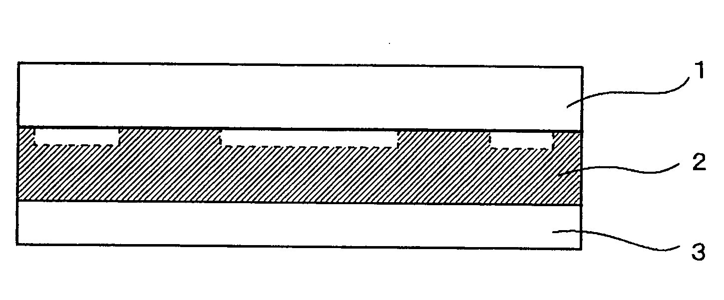
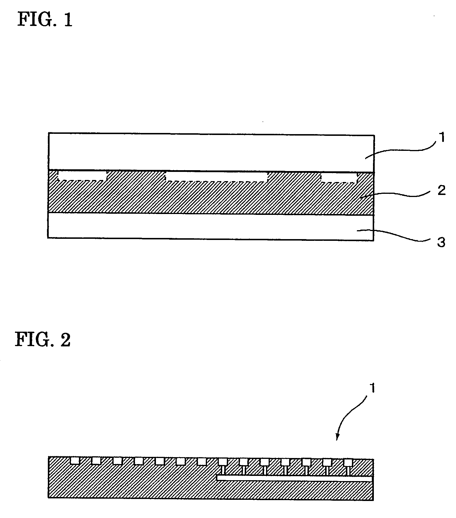
[0064]The materials shown in Table 1 were prepared with a thickness of 12 mm and a diameter of 310 mm. Grooves as shown in FIG. 1 were formed thereon, and holes connecting the grooves were then machined. The surfaces were then plated with nickel, and the side containing the wafer-mounting surface was ground to a mirror finish with a flatness of 5 μm and a surface roughness Ra of 0.1 μm or less, resulting in a chuck top.

TABLE 1ThermalYoung'sconductivitymodulusMaterial(W / mK)(GPa)1Copper3901202Aluminum230803Al—SiC1501304Aluminum nitride1702705Silicon nitride25300

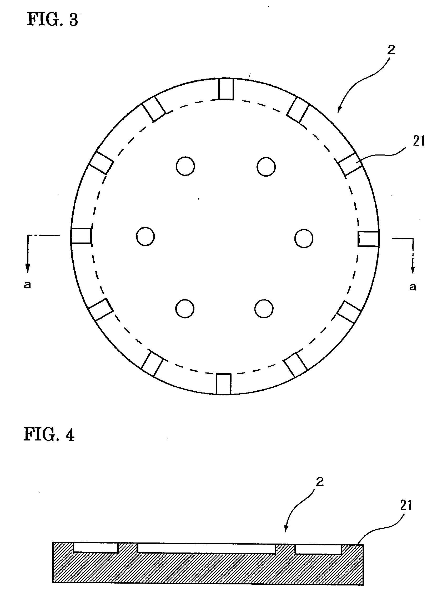
[0065]The materials shown in Table 2 were prepared with a thickness of 15 mm and a diameter of 310 mm to serve as support members. The upper and lower surfaces of these materials were polished and processed until the flatness and parallelism were each 10 μm or less. Then counter-sinks having a depth of 5 mm were formed in the shape shown in FIG. 3 and FIG. 4, resulting in a support member. Metal materials were cast and then fin...


PUM

PropertyMeasurementUnit
Young's modulus Y3aaaaaaaaaa
thicknessaaaaaaaaaa
Young's modulusaaaaaaaaaa

Abstract

A wafer holder is provided having high rigidity and an enhanced heat-insulating effect that allow positional accuracy and heating uniformity to be improved, a chip to be rapidly heated and cooled, and the manufacturing cost to be reduced, and a wafer prober apparatus on which the wafer holder is mounted. The wafer holder of the present invention includes a chuck top for mounting a wafer, a support member for supporting the chuck top, and a stand for supporting the support member. The chuck top has a thermal conductivity K1 and a Young's modulus Y1; the support member has a thermal conductivity K2 and a Young's modulus Y2; and the stand has a thermal conductivity K3 and a Young's modulus Y3. K1>K2 and K1>K3; and Y3>Y1 and Y3>Y2.

Description

BACKGROUND OF THE INVENTION[0001]1. Field of the Invention[0002]The present invention relates to a wafer holder having exceptional rigidity and heating uniformity, and in particular relates to a wafer holder and a heater unit used in a wafer prober for mounting a semiconductor wafer on a wafer-mounting surface and pressing a probe card against the wafer to inspect the electrical characteristics of the water, and to a wafer prober on which the wafer holder and the heater are mounted.[0003]2. Description of the Background Art[0004]In the prior art, a heating procedure is performed in a semiconductor inspection step on a semiconductor substrate (wafer) to be treated. Specifically, the wafer is heated to a temperature higher than the normal operating temperature, potentially defective semiconductor chips are made to fail at an accelerated rate and are removed, and a burn-in is performed to prevent the occurrence of defects after shipping. In the burn-in step, after the semiconductor cir...

Claims


Application Information

Patent Timeline
Patent Type & Authority Applications(United States)
IPC IPC(8): G01R31/02
CPCH01L21/68757G01R31/2865
Inventor NATSUHARA, MASUHIROAWAZU, TOMOYUKINAKATA, HIROHIKOITAKURA, KATSUHIRO
Owner SUMITOMO ELECTRIC IND LTD
Why Eureka
Try Eureka