Electrostatic chuck member, method of manufacturing the same, and electrostatic chuck device

a technology of electrostatic chuck and chuck member, which is applied in the direction of electrostatic holding device, manufacturing tools, mechanical apparatus, etc., can solve the problems of poor reliability and yield of electrostatic chuck, complicated structure of electrostatic chuck, etc., to suppress the generation of particles, improve dechuck operation, and eliminate drawbacks

Inactive Publication Date: 2009-03-05
SHINKO ELECTRIC IND CO LTD
View PDF0 Cites 293 Cited by
  • Summary
  • Abstract
  • Description
  • Claims
  • Application Information

AI Technical Summary

Benefits of technology

[0011]The invention has been made in consideration of the problems of the conventional electrostatic chuck having an emboss and has an object to provide an improved electrostatic chuck member which can cope with ultrafining of a semiconductor device and can improve effects derived from the emboss, for example, a soaking property during a wafer processing and a dechuck operation after the processing and can avoid the generation of a particle without causing a structure of an electrostatic chuck and a manufacturing process from being complicated.
[0012]Moreover, it is an object of the invention to provide a method capable of easily manufacturing the improved electrostatic chuck member without damaging a reliability, a yield and a productivity.
[0013]Furthermore, it is an object of the invention to provide an improved electrostatic chuck device having no problem caused by an electrostatic chuck when it is used in a manufacture of a semiconductor device.
[0047]According to the invention, as will be understood from the following detailed description, the edge part is broken in the protruded portion formed on the electrostatic chuck surface and is thus rounded so that the surface is smoothed. Thus, it is possible to eliminate a drawback that the semiconductor wafer is caught on the edge part. Accordingly, it is possible to suppress the generation of the particles.
[0048]As a result, according to the invention, it is possible to cope with ultrafining of a wiring rule, to control a wafer temperature in the process and to achieve a soaking property during the wafer processing, and furthermore, to improve a dechuck operation after the wafer processing in the manufacture of the semiconductor device. In addition, the structure of the electrostatic chuck according to the invention is not complicated. Therefore, it is possible to easily manufacture the semiconductor device without deteriorating a reliability, a yield and a productivity.

Problems solved by technology

In case of the method, however, a structure of an electrostatic chuck is complicated and a poor reliability and yield of the electrostatic chuck is obtained.[Patent Document 1] JP-A-2000-277594 (Summary and Claims)[Patent Document 2] JP-A-2003-264223 (Summary and Claims)[Patent Document 3] JP-A-2004-253402 (Summary and Claims)

Method used


Image

  • Electrostatic chuck member, method of manufacturing the same, and electrostatic chuck device
  • Electrostatic chuck member, method of manufacturing the same, and electrostatic chuck device
  • Electrostatic chuck member, method of manufacturing the same, and electrostatic chuck device

Examples


example 1

[0098]In the example, an electrostatic chuck member having a protruded portion is fabricated by a method of smoothing, through wrapping using a free abrasive grain, an edge part of the protruded portion formed on a surface of the electrostatic chuck member through embossing.

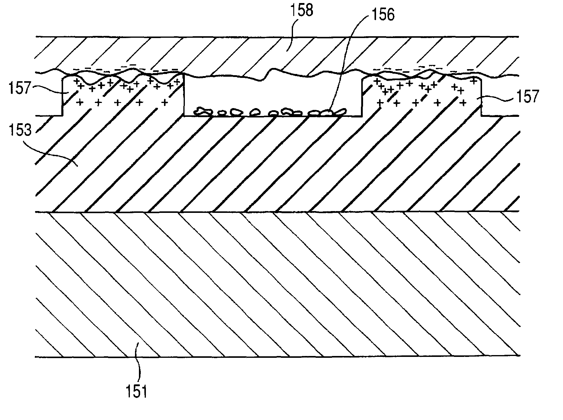
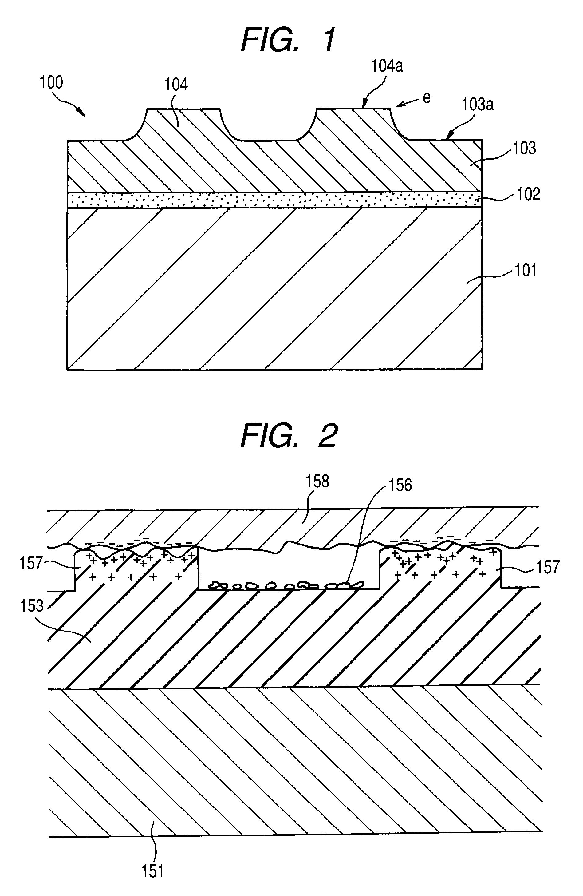
[0099]There is prepared the electrostatic chuck member formed of alumina ceramic which is fabricated in the comparative example 1. The electrostatic chuck member had a diameter of 300 mm and a thickness of 1 mm and included 360 protruded portions having a diameter of 1 mm and a height of 0.01 mm in total.

[0100]Subsequently, the surface of the electrostatic chuck member is subjected to the wrapping using a free abrasive grain. In the example, a wrapping machine put on the market is used and an edge part of the protruded portion is processed by a softer grinding material than the electrostatic chuck member. The grinding material used herein is an alumina based abrasive grain. In order to vary a size (mm) of a round...

example 2

[0102]In the example, an electrostatic chuck member having a protruded portion is fabricated by a method of smoothing, through blasting, an edge part of the protruded portion formed on a surface of the electrostatic chuck member through embossing.

[0103]There is prepared the electrostatic chuck member formed of alumina ceramic which is fabricated in the comparative example 1. The electrostatic chuck member had a diameter of 300 mm and a thickness of 1 mm and included 360 protruded portions having a diameter of 1 mm and a height of 0.01 mm in total.

[0104]In order to cause a mirror surface formed on a surface of the protruded portion to protect a surface to be processed, subsequently, a mask having a diameter of 0.5 mm which is smaller than an embossing diameter is laminated on an embossed surface. The mask used in the example is a mask sheet formed by the same material as that used in the formation of the protruded portion in the comparative example 1. An edge part of the protruded po...

example 3

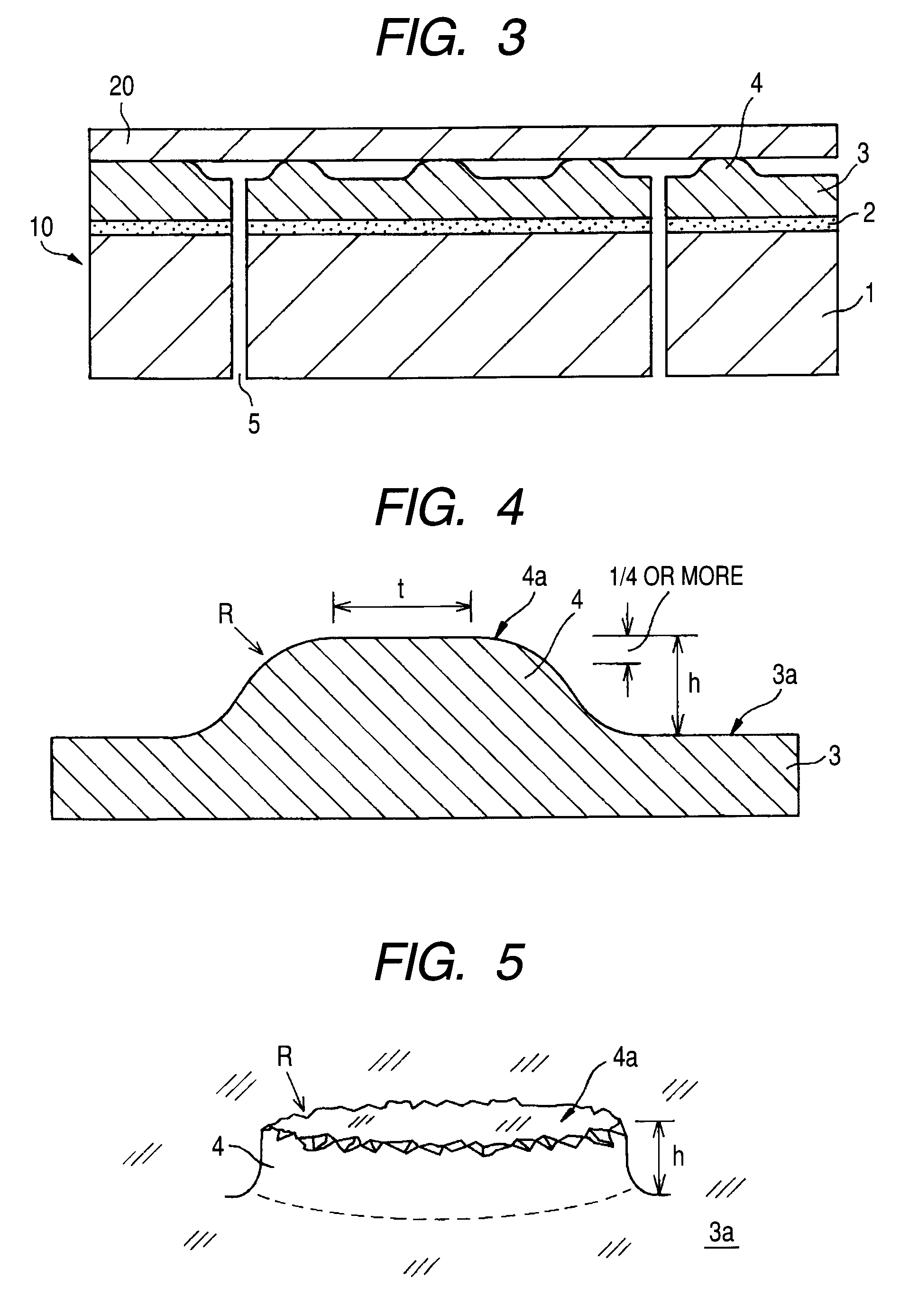
[0106]In the example, an electrostatic chuck member having a protruded portion is fabricated by a method of smoothing the protruded portion through embossing so as to break an edge part in the embossing when forming the protruded portion on a surface of the electrostatic chuck member through the embossing.

[0107]There is prepared the mask sheet fabricated in the comparative example 1. The mask sheet is a positive type acrylic resin film in a thickness of 50 μm which includes, as a support film, a PET film in a thickness of 80 μm. The resin film is formed in a positive pattern corresponding to the protruded portion of the electrostatic chuck member.

[0108]According to the technique described above with reference to FIGS. 7A to 7D, next, the electrostatic chuck member having a protruded portion is fabricated in accordance with the invention. The electrostatic chuck member prepared in the example is laminated on a substrate formed of aluminum having a diameter of 300 mm and a thickness o...


PUM

PropertyMeasurementUnit
heightaaaaaaaaaa
diameteraaaaaaaaaa
grain sizeaaaaaaaaaa

Abstract

A plurality of protruded portions is formed through embossing and is distributed and arranged regularly or irregularly on an electrostatic chuck surface, and has a circular or almost circular top surface shape and a roundness (R) of 0.01 mm or more is applied to an edge part defined by an intersection of the top surface and a side surface and a portion to which the roundness is applied occupies a quarter of a height h of the protruded portion or more.

Description

BACKGROUND OF THE INVENTION[0001]The present invention relates to an electrostatic chuck member and an electrostatic chuck device, and more particularly to an electrostatic chuck member to be used for holding and fixing a substance to be processed such as a semiconductor wafer by utilizing an electrostatic chucking force in a manufacture of a semiconductor device and an electrostatic chuck device including the electrostatic chuck member. The invention also relates to a method of manufacturing the electrostatic chuck member.[0002]In a manufacture of a semiconductor device, as is well known, a semiconductor wafer formed of silicon is subjected to various processings such as etching and sputtering with the semiconductor wafer fixed by a chuck device in a processing apparatus when the semiconductor wafer is to be processed, for example. In the chuck device, means for holding and fixing the semiconductor wafer includes means for utilizing a mechanical fixing force and means for utilizing...

Claims


Application Information

Patent Timeline
Patent Type & Authority Applications(United States)
IPC IPC(8): H02N13/00H01L21/67B23B31/28
CPCH01L21/6833H02N13/00Y10T29/5313Y10T279/23Y10T29/49002Y10T29/53174
Inventor KOBAYASHI, HIROYUKI
Owner SHINKO ELECTRIC IND CO LTD
Why Eureka
Try Eureka