Semiconductor package and semiconductor device

a semiconductor and semiconductor technology, applied in the field of semiconductor devices, can solve the problems of high mold cost and dramatic increase in production cost, and achieve the effect of reducing production cos

Inactive Publication Date: 2008-03-27
ADVANCED SEMICON ENG INC
View PDF22 Cites 212 Cited by
  • Summary
  • Abstract
  • Description
  • Claims
  • Application Information

AI Technical Summary

Benefits of technology

[0009]Another objective of the present invention is to provide a semiconductor package, which comprises a substrate, a chip, a plurality of connecting elements, a plurality of first conductive bodies, and a molding compound. The substrate has a first surface and a second surface. The chip is attached to the first surface of the substrate. The connecting elements electrically connect the chip and the substrate. The first conductive bodies are disposed on the first surface of the substrate. The molding compound encapsulates the first surface of the substrate, the chip, the connecting elements, and the first conductive bodies. The molding compound has at least two heights and one end of each of the first conductive bodies is exposed. Thereby, the molding compound encapsulates the entire first surface of the substrate, and the pads on the first surface will not be polluted.
[0010]Still another objective of the present invention is to provide a semiconductor device, which comprises a first package and a second package. The first package is the semiconductor package as described above. The second package is stacked on the first package. In an embodiment, the size of the second package is the same as that of the first package. Thus, only one mold is required to perform both the molding processes for the second package and the first package. Accordingly, the production cost will be reduced.

Problems solved by technology

The cost is high for making a mold.
Accordingly, the production cost will be dramatically increased.

Method used


Image

  • Semiconductor package and semiconductor device
  • Semiconductor package and semiconductor device
  • Semiconductor package and semiconductor device

Examples


Embodiment Construction

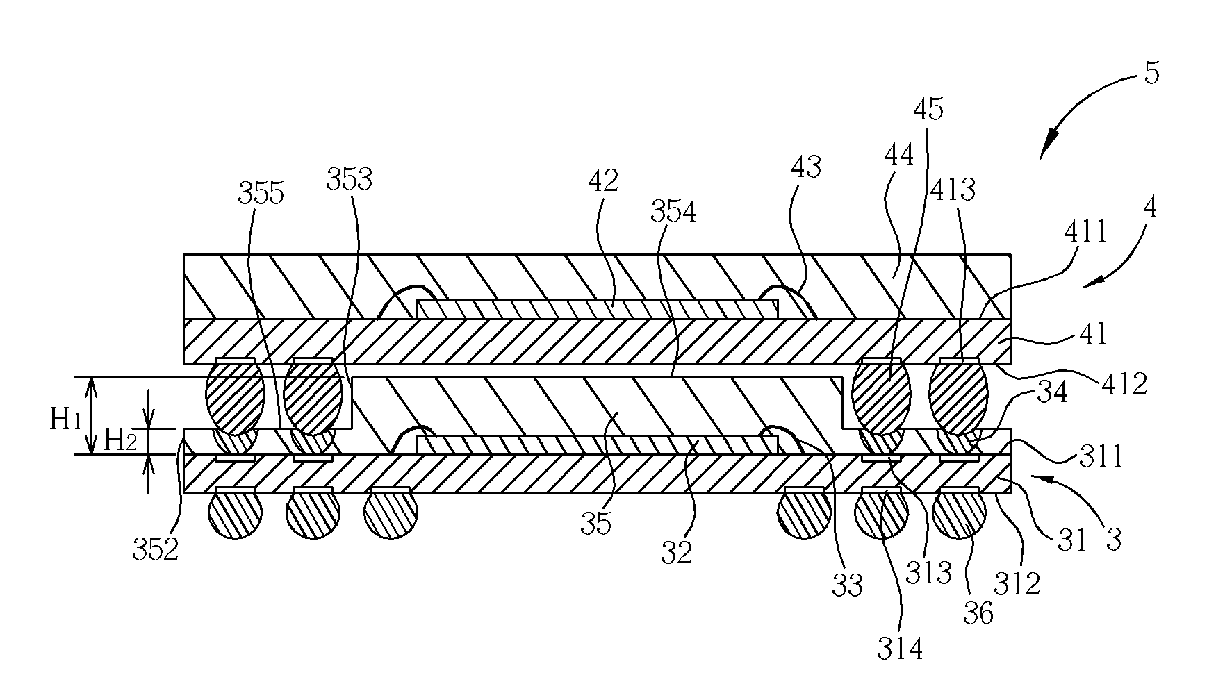
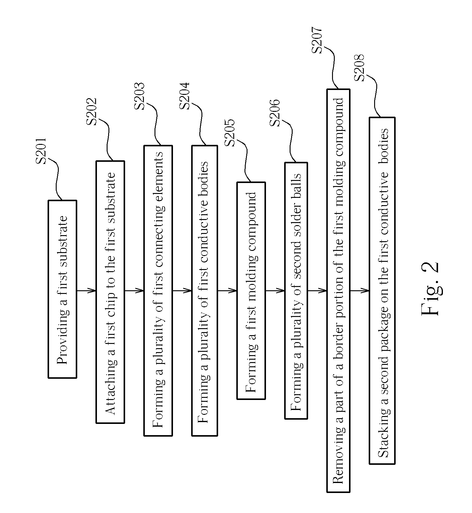
[0015]Please refer to FIG. 2 showing a flow chart of the method of making a semiconductor device according to the present invention. Also refer to FIG. 3. In Step S201, a first substrate 31 is provided. The first substrate 31 has a first surface 311, a second surface 312, a plurality of first pads 313, and a plurality of second pads 314. The first pads 313 are on the first surface 311, and the second pads 314 are on the second surface 312. In Step S202, a first chip 32 is attached to the first surface 311 of the first substrate 31. In this embodiment, a first chip 32 is attached to the first surface 311 of the first substrate 31. In Step S203, a plurality of first connecting elements (such as a plurality of first conductive wires 33) electrically connect the first chip 32 and the first surface 311 of the first substrate 31. In Step 204, a plurality of first conductive bodies (such as a plurality of first solder balls 34) are formed on the first pads 313 on the first surface 311 of t...


PUM


Abstract

The present invention relates to a semiconductor package and a semiconductor device and a method of making the same. The method of making the semiconductor package comprises: providing a substrate; attaching a chip to a surface of the substrate; forming a plurality of connecting elements for electrically connecting the chip and the substrate; forming a plurality of first conductive bodies on the surface of the substrate; forming a molding compound for encapsulating the surface of the substrate, the chip, the connecting elements and the first conductive bodies; and removing a part of a border portion of the molding compound, so that the molding compound has two heights and one end of each first conductive bodies is exposed. Thereby, the molding compound covers the entire surface of the substrate, so that the bonding pads on the surface of the substrate will not be polluted.

Description

BACKGROUND OF THE INVENTION[0001]1. Field of the Invention[0002]The present invention relates to a semiconductor package and a method of making the same, and particularly to a semiconductor package comprising a molding compound with different heights and a semiconductor device comprising the semiconductor package and methods of making the same.[0003]2. Description of the Prior Art[0004]Please refer to FIG. 1 showing a schematic diagram of a conventional semiconductor device consisting of stacked packages. The conventional semiconductor device 1 comprises a first package 10 and a second package 20. The first package 10 comprises a first substrate 11, a first chip 12, a plurality of first conductive wires 13, a first molding compound 14, and a plurality of first solder balls 15. The first substrate 11 has an upper surface 111, a lower surface 112, and a plurality of first pads 113. The first pads 113 are disposed on the upper surface 111 of the first substrate 11. The first chip 12 is...

Claims


Application Information

Patent Timeline
Patent Type & Authority Applications(United States)
IPC IPC(8): H01L23/02H01L23/52
CPCH01L21/56H01L2224/1405H01L23/49816H01L25/105H01L25/50H01L2224/48091H01L2224/48227H01L2924/01079H01L2924/15331H01L23/3128H01L24/14H01L2924/1815H01L2924/15321H01L2224/73265H01L2224/32225H01L2225/1023H01L2225/1058H01L24/48H01L2924/00014H01L2924/00012H01L2924/181H01L2924/12042H01L24/73H01L2924/00H01L2224/45099H01L2224/45015H01L2924/207
Inventor WU, YEN-YISUNG, WEI-YUEHCHANG CHIEN, PAO-HUEICHU, CHI-CHIHLEE, CHENG-YINWENG, GWO-LIANG
Owner ADVANCED SEMICON ENG INC
Why Eureka
Try Eureka