Deposition Donor Substrate and Method for Manufacturing Light-Emitting Device

a donor substrate and light-emitting technology, applied in the direction of transportation and packaging, vacuum evaporation coating, coating, etc., can solve the problem of transfer of the entire transfer layer, and achieve the effect of reducing the manufacturing cost of the deposition donor substrate, high definition, and easy and accurate formation

Inactive Publication Date: 2010-01-21
SEMICON ENERGY LAB CO LTD
View PDF13 Cites 41 Cited by
  • Summary
  • Abstract
  • Description
  • Claims
  • Application Information

AI Technical Summary

Benefits of technology

[0023]According to a deposition donor substrate of an embodiment of the present invention, since the partition layer has an inverse taper shape and thus there is a space between the partition layer and the light-absorbing layer, heat conduction from the light-absorbing layers to the partition layers can be suppressed, so that the material layers that are formed on the partition layers can be prevented from being heated. This makes it possible to sublime only the material layers in regions overlapped with the light-absorbing layers so that an EL layer having a desired pattern can be formed over the second substrate.
[0024]Further, according to a deposition donor substrate of an embodiment of the present invention, because of the difference in thickness between the light-absorbing layer and the partition layer and further because of the inverse taper shape of the partition layer, the material layers or the reflective layers can be formed so that they are separated from each other. Therefore, the material layers or the reflective layers can be formed to have a desired pattern. Accordingly, it is not necessary to perform a photolithography process that is generally required to form a pattern over a deposition donor substrate, which results in a reduction in manufacturing costs of the deposition donor substrate.
[0025]In addition, by using a deposition donor substrate of an embodiment of the present invention, the thickness of a film formed over a deposition target substrate can be controlled by controlling the thicknesses of the material layers formed in the deposition donor substrate. Therefore, a practitioner does not need to adjust the evaporation rate by using a thickness monitor, and thus the deposition process can be fully automated.
[0026]Furthermore, by using a deposition donor substrate of an embodiment of the present invention, an EL layer-forming ...

Problems solved by technology

Such heat conduction in the plane direction of the photothermal conversion lay...

Method used


Image

  • Deposition Donor Substrate and Method for Manufacturing Light-Emitting Device
  • Deposition Donor Substrate and Method for Manufacturing Light-Emitting Device
  • Deposition Donor Substrate and Method for Manufacturing Light-Emitting Device

Examples


embodiment 1

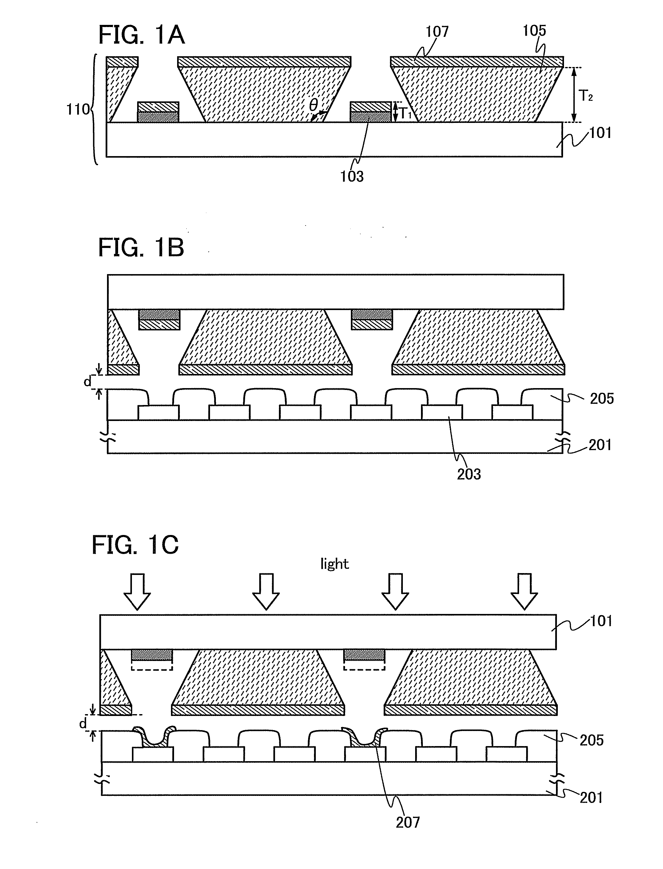
[0042]A deposition donor substrate and a method for manufacturing a light-emitting device according to Embodiment 1 will be described using FIGS. 1A to 1C.

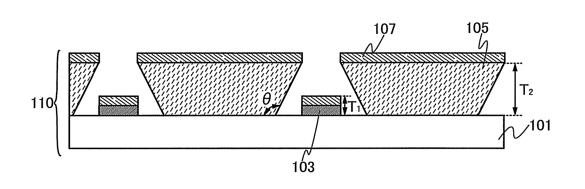
[0043]FIG. 1A illustrates an example of a deposition donor substrate 110 according to Embodiment 1. In FIG. 1A, on a first substrate 101 which is a supporting substrate, a plurality of light-absorbing layers 103 which are island shaped or stripe shaped are provided so that they are separated from each other. Further, partition layers 105 are each formed between the light-absorbing layers 103. Furthermore, material layers 107 are formed on the light-absorbing layers 103 and on the partition layers 105 so that the material layers 107 are separated from each other.

[0044]A method for manufacturing a deposition donor substrate according to Embodiment 1 which is illustrated in FIG. 1A and a method for manufacturing a light-emitting device by using the deposition donor substrate will be described.

[0045]First, the light-absorbing layers a...

embodiment 2

[0086]In Embodiment 2, a deposition donor substrate which differs in structure from the deposition donor substrate in the above Embodiment 1 will be described. Note that the deposition donor substrate described in Embodiment 2 is formed using a material and a manufacturing method that are similar to those of Embodiment 1 if not otherwise stated.

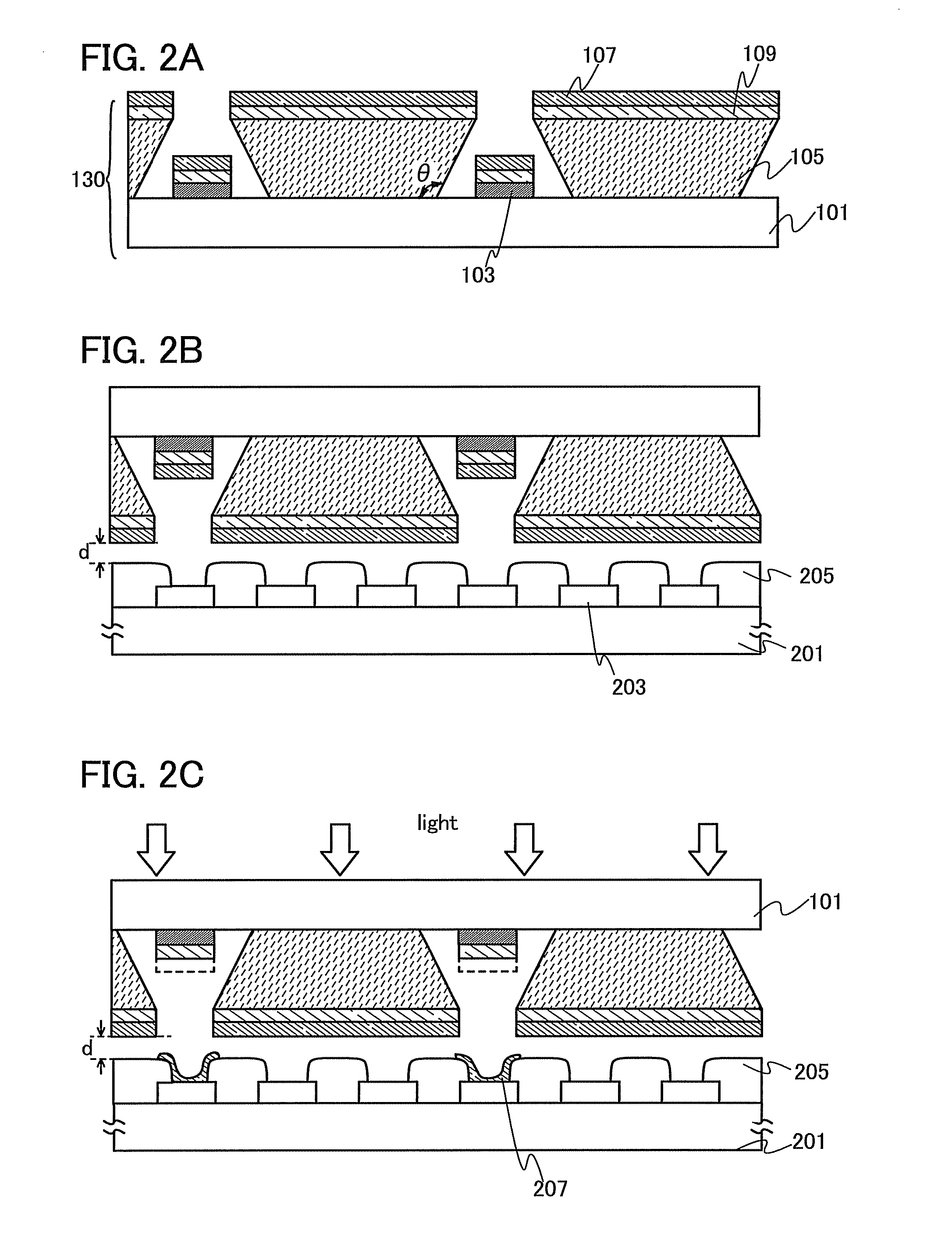
[0087]FIG. 2A illustrates an example of a deposition donor substrate 130 according to Embodiment 1. In FIG. 2A, on the first substrate 101 which is a supporting substrate, the light-absorbing layers 103 which are island shaped or stripe shaped are provided so that they are separated from each other. Further, the partition layers 105 are each formed between the light-absorbing layers 103. Furthermore, reflective layers 109 are formed on the light-absorbing layers 103 and on the partition layers 105. The material layers 107 to which an EL layer-forming material is attached are formed on the light-absorbing layers 103 and on the partition layers...

embodiment 3

[0104]In Embodiment 3, a method for manufacturing a light-emitting device capable of full-color display by forming EL layers of light-emitting elements by using a plurality of deposition donor substrates described in Embodiment 1 or 2 will be described.

[0105]First, three deposition donor substrates described in Embodiment 1 or 2 are prepared. The deposition donor substrates used in Embodiment 3 are as described with reference to FIGS. 1A to 1C in Embodiment 1. Note that the deposition donor substrates are each provided with material layers in order that EL layer-forming materials included in the material layers form EL layers that exhibit light emission of different colors. Specifically, a first deposition donor substrate provided with material layers (R) including an EL layer-forming material for forming an EL layer that exhibits red light emission (an EL layer (R)), a second deposition donor substrate provided with material layers (G) including an EL layer-forming material for for...


PUM

PropertyMeasurementUnit
Thicknessaaaaaaaaaa
Thicknessaaaaaaaaaa
Thicknessaaaaaaaaaa

Abstract

One surface of a first substrate provided with at least light-absorbing layers separately formed, partition layers each formed between the light-absorbing layers and having an inverse taper shape, and material layers formed on the light-absorbing layers and on the partition layers so that the material layers are separated from each other is disposed to face a deposition target surface of a second substrate; light irradiation is performed from the other surface of the first substrate, only the material layers in regions overlapped with the light-absorbing layers are heated and evaporated to the deposition target surface of the second substrate.

Description

BACKGROUND OF THE INVENTION[0001]1. Field of the Invention[0002]The present invention relates to a deposition donor substrate used for deposition of a material that can be deposited by an evaporation method and a method for manufacturing a light-emitting device using the deposition donor substrate.[0003]2. Description of the Related Art[0004]Light-emitting elements, which use organic compounds as a light emitter and are characterized by the thinness, lightweight, fast response, and direct current low voltage driving, are expected to be applied to next-generation flat panel displays. In particular, display devices having light-emitting elements arranged in matrix are thought to be superior to conventional liquid crystal display devices for their wide viewing angles and excellent visibility.[0005]As for a light-emitting mechanism of a light-emitting element, an EL layer is interposed between a pair of electrodes and voltage is applied, whereby electrons injected from a cathode and hol...

Claims


Application Information

Patent Timeline
IPC IPC(8): B32B7/02B29C71/02
CPCH01L51/56H01L51/0013Y10T428/24975Y10T428/2495C23C14/048H10K71/18H10K71/00
Inventor SEO, SATOSHIYOKOYAMA, KOHEI
Owner SEMICON ENERGY LAB CO LTD
Why Eureka
Try Eureka