Pixel driving circuit, compensation method thereof and display panel

A technology of pixel drive circuit and capacitor circuit, which is applied in the direction of static indicators and instruments, can solve the problems of large number of TFTs, limited high-resolution display design, and large design space, so as to improve PPI, improve display effect, The effect of eliminating influence

Active Publication Date: 2022-03-18
CHANGSHA HKC OPTOELECTRONICS CO LTD +1
View PDF11 Cites 1 Cited by
  • Summary
  • Abstract
  • Description
  • Claims
  • Application Information

AI Technical Summary

Problems solved by technology

Therefore, it is derived that each pixel usually uses an 8T1C pixel circuit composed of eight transistors and a capacitor, but this design has a large number of TFTs and takes up a large design space, which limits the design of high-resolution displays to a certain extent.

Method used


Image

  • Pixel driving circuit, compensation method thereof and display panel
  • Pixel driving circuit, compensation method thereof and display panel
  • Pixel driving circuit, compensation method thereof and display panel

Examples


Embodiment Construction

[0031] It should be understood that the terminology and specific structural and functional details disclosed herein are representative only for describing specific embodiments, but the application can be embodied in many alternative forms and should not be construed as merely Be limited by the examples set forth herein. In the description of the present application, the terms "first" and "second" are used for descriptive purposes only, and cannot be understood as indicating relative importance, or implicitly indicating the quantity of indicated technical features. Therefore, unless otherwise stated, the features defined as "first" and "second" may explicitly or implicitly include one or more of these features; Understand the specific meanings of the above terms in this application.

[0032] The present application will be described in detail below with reference to the accompanying drawings and optional embodiments.

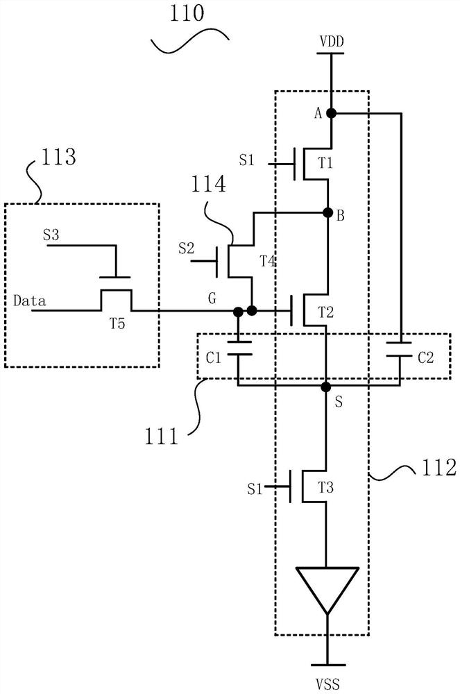
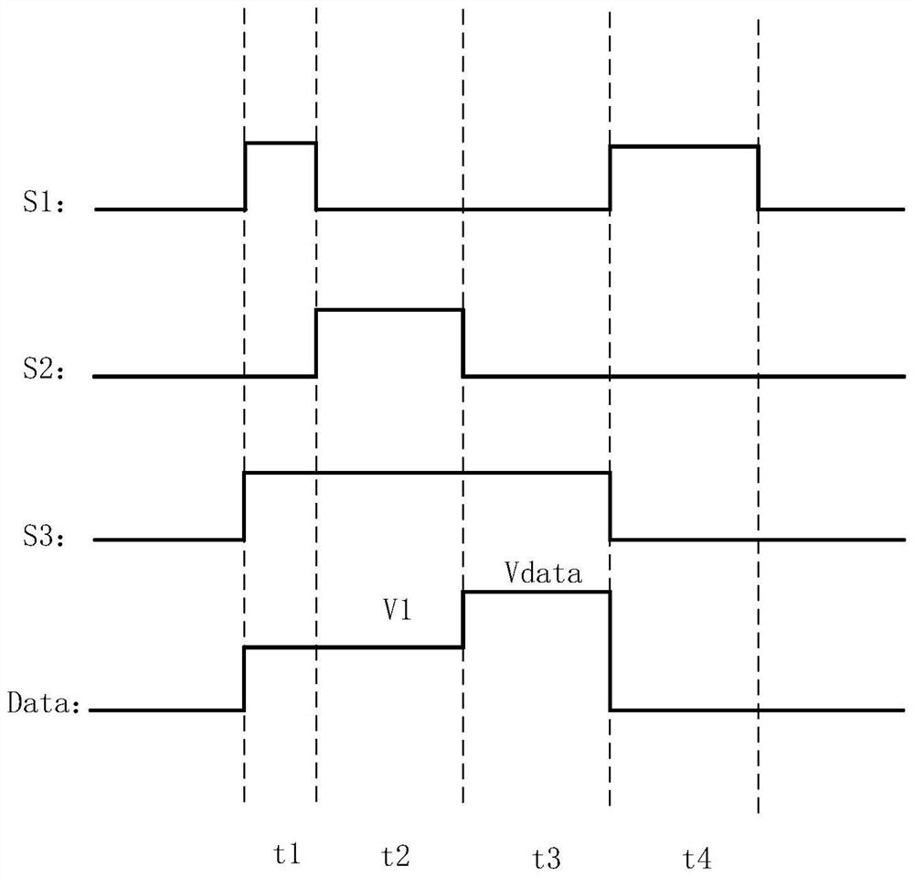
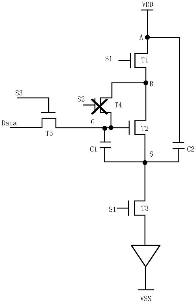
[0033] Such as figure 1 as shown, figure 1A schematic d...


PUM


Abstract

The invention discloses a pixel driving circuit, a compensation method thereof and a display panel. The pixel driving circuit comprises a capacitance circuit, a light emitting circuit, a data input circuit and a compensation circuit. The capacitance circuit stores the voltage of the first node, the voltage of the second node and the voltage of the third node; the light-emitting circuit is connected with a first control signal and emits light under the control of the first control signal and the voltage of the first node; the data input circuit accesses a third control signal and a data signal, and transmits the data signal to the first node under the control of the third control signal; and the compensation circuit accesses a second control signal, transmits the voltage of the first node to the fourth node under the control of the second control signal, and performs compensation charging on the second node through the voltage of the fourth node under the control of the voltage of the first node. By providing the simpler pixel driving circuit, the technical problem that the existing pixel driving circuit is relatively complex in structure and occupies a large area during layout design is solved.

Description

technical field [0001] The present application relates to the field of display technology, and in particular to a pixel driving circuit, a compensation method thereof, and a display panel. Background technique [0002] OLED (Organic Light-Emitting Diode) display has many advantages such as thin body, power saving, bright color, and high image quality, and has been widely used. Such as OLED TVs, mobile phones, notebook computers, etc., gradually occupy a dominant position in the field of flat panel display. [0003] Among them, in the OLED display panel, the pixels are arranged in a matrix including multiple rows and columns. The earliest pixel design adopts that each pixel is usually composed of two transistors (T) and a capacitor (C), also known as It is a 2T1C pixel circuit, but the transistor has the problem of threshold voltage drift. Therefore, it is derived that each pixel usually uses an 8T1C pixel circuit consisting of eight transistors and a capacitor, but this de...

Claims


Application Information

Patent Timeline
Patent Type & Authority Applications(China)
IPC IPC(8): G09G3/3208G09G3/3291
CPCG09G3/3208G09G3/3291G09G2320/0257
Inventor 卢昭阳李荣荣
Owner CHANGSHA HKC OPTOELECTRONICS CO LTD
Why Eureka
Try Eureka