Display substrate and manufacturing method thereof and display device

A technology for display substrates and substrates, which is applied in the direction of image reproducers, static indicators, and picture replicators of solid-state color display devices, and can solve the problems of sub-pixel display brightness and chromaticity deviation, display screen flicker, time inconsistency, etc. , to achieve the effect of improving display quality, improving screen flicker, and improving user experience.

Pending Publication Date: 2020-12-01
BOE TECH GRP CO LTD +1
View PDF0 Cites 5 Cited by
  • Summary
  • Abstract
  • Description
  • Claims
  • Application Information

AI Technical Summary

Problems solved by technology

[0004] The object of the present invention is to provide a display substrate and its manufacturing method, and a display device, which are used to solve the problem that the brightness and chromaticity displayed by the sub-pixel during t

Method used


Image

  • Display substrate and manufacturing method thereof and display device
  • Display substrate and manufacturing method thereof and display device
  • Display substrate and manufacturing method thereof and display device

Examples


Example Embodiment

[0064] In order to further illustrate a display substrate, a manufacturing method thereof, and a display device provided by the embodiments of the present invention, the following detailed description is given with reference to the accompanying drawings.

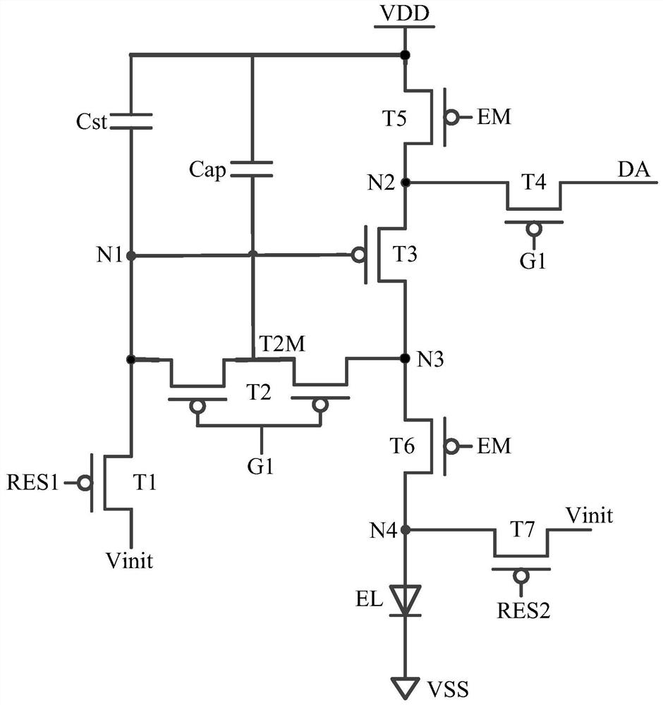
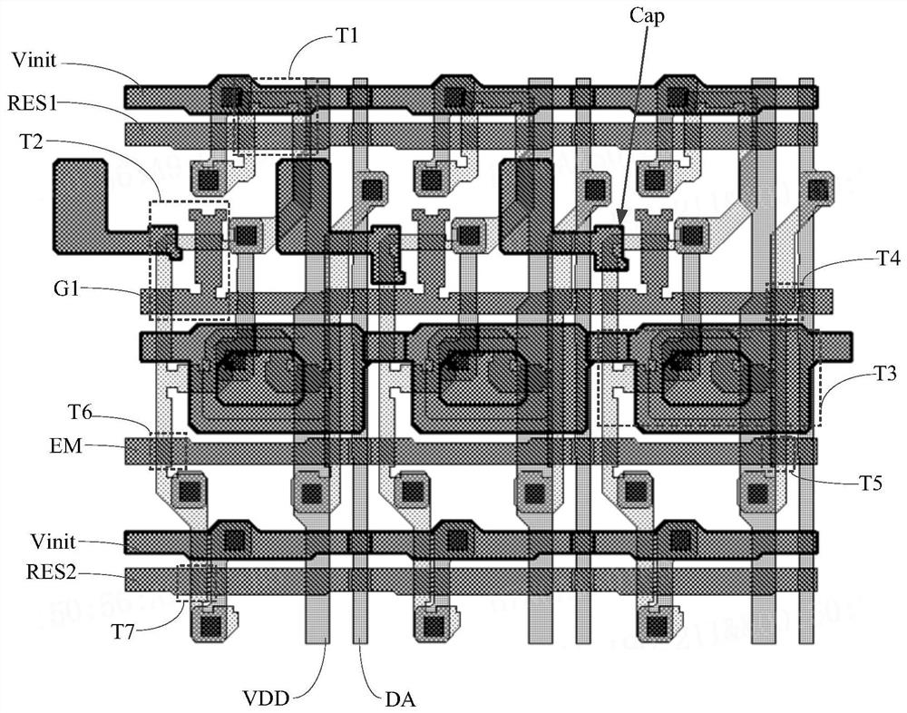
[0065] like figure 1 and image 3 As shown, the display substrate provided by the embodiment of the present invention includes a plurality of sub-pixels, each sub-pixel includes a sub-pixel driving circuit, and the sub-pixel driving circuits included in the plurality of sub-pixels are distributed on the base of the display substrate in an array. Each sub-pixel driving circuit includes first to seventh transistors T1 to T7, and a storage capacitor Cst. The second transistor T2 serves as a compensation transistor in the sub-pixel driving circuit, and the third transistor T3 serves as a driving transistor in the sub-pixel driving circuit. The compensation transistor has a double gate structure, the first electrode of the comp...


PUM


Abstract

The invention provides a display substrate and a manufacturing method thereof and a display device, relates to the technical field of display, and aims to solve the problem that screen flickering of adisplay occurs due to inconsistent time for anode voltage in sub-pixels of different colors to reach stability. In the display substrate, each sub-pixel comprises a power supply signal line, a sub-pixel driving circuit and a shielding pattern; the sub-pixel driving circuit comprises a driving transistor and a compensation transistor with a double-gate structure; the shielding pattern is electrically connected with the power signal lines in the adjacent sub-pixels in the second direction, and an overlapping area exists between the orthographic projection of the shielding pattern on the substrate and the orthographic projection of the conductor pattern in the compensation transistor on the substrate; the display substrate comprises a plurality of first sub-pixels and a plurality of second sub-pixels, and the overlapping area in the first sub-pixels is larger than that in the second sub-pixels. The display substrate provided by the invention is used for displaying.

Description

technical field [0001] The invention relates to the field of display technology, in particular to a display substrate, a manufacturing method thereof, and a display device. Background technique [0002] Active Matrix Organic Light-Emitting Diode (English: Active Matrix Organic Light-Emitting Diode, referred to as: AMOLED,) display, compared with the traditional liquid crystal display, has the advantages of self-illumination, wide color gamut, high contrast, light and thin, etc., and has been widely used in recent years. Applied in various fields. [0003] The AMOLED display includes a sub-pixel driving circuit, and the gate voltage of the driving transistor in the sub-pixel driving circuit is easily interfered by other transistors, and is in an unstable state during the light-emitting phase. The instability of the gate voltage of the drive transistor will cause the anode voltage of the light-emitting element to change, so that the anode voltage of the light-emitting element...

Claims


Application Information

Patent Timeline
IPC IPC(8): G09G3/3225H01L27/32
CPCG09G3/3225H10K59/1216G09G2300/0852G09G2300/0819G09G3/3233G09G2310/061G09G2300/0861G09G2300/0426H01L27/124H10K59/35H10K59/126H10K59/131H04N9/30H10K71/00H10K59/1201
Inventor 杨慧娟姜晓峰
Owner BOE TECH GRP CO LTD
Why Eureka
Try Eureka