Display panel and display device

A display panel and display area technology, which is applied to TVs, color TVs, electric solid-state devices, etc., can solve the problems of obvious dividing lines, reduced screen ratio, and damage to the overall consistency of the display panel, so as to ensure the overall consistency and improve the The effect of screen ratio

Active Publication Date: 2020-12-29
WUHAN TIANMA MICRO ELECTRONICS CO LTD
View PDF10 Cites 2 Cited by
  • Summary
  • Abstract
  • Description
  • Claims
  • Application Information

AI Technical Summary

Problems solved by technology

[0004] In order to solve the above technical problems, the present application provides a display panel and a display device to solve the problems that the overall consistency of the display panel is destroyed and the screen-to-body ratio is reduced by setting a non-display area to avoid optical elements. There is an obvious boundary between the transparent display area of ​​the component and the adjacent display area

Method used


Image

  • Display panel and display device
  • Display panel and display device
  • Display panel and display device

Examples


Embodiment Construction

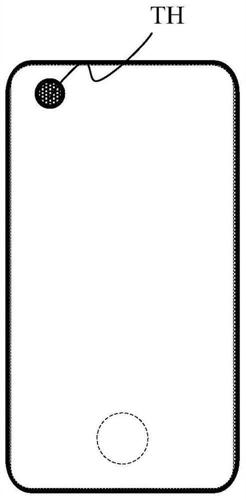
[0030] As mentioned in the Background Art, refer to figure 1 , figure 1 It is a top view schematic diagram of a display panel in the prior art. In order to set up optical elements such as a front camera, the existing design usually leaves a light-transmitting area TH for the optical elements by digging holes or digging grooves on the front of the display screen, so that the optical elements Normal work can be performed using the light passing through the light-transmitting region TH. but from figure 1 It can be clearly seen from the figure that these grooves or hole-digging areas cannot be used for display, causing damage to the overall consistency of the display panel, and due to the existence of the grooves or hole-digging areas, a true full screen cannot be realized.

[0031] In order to solve this problem, the inventors have found through research that the purpose of light transmission for optical elements can be achieved by reducing the pixel density in a certain area o...


PUM


Abstract

The invention discloses a display panel and a display device. A substrate of the display panel comprises a first display area, a second display area and a third display area, pixel density in the first display area can be set to be low so as to meet a light transmission requirement of an optical element, a non-display area does not need to be arranged for the optical element, and a screen-to-bodyratio of the display panel can be increased; and the overall consistency of the display panel is ensured. In addition, the pixel density of the display pixels in the second display area is decreased progressively in the first direction so that a problem of display screen splitting caused by an abrupt change of the pixel density from the third display area to the first display area is solved. Furthermore, an aperture opening ratio of the display pixels in the second display area is gradually increased along the first direction so that the current density of the display pixels in the area with lower pixel density is favorably ensured not to be too high under the condition of ensuring the display brightness consistency of each area of the second display area; and adverse effects on the service life of the display pixels caused by the over-high current density are avoided.

Description

technical field [0001] The present application relates to the field of display technology, and more specifically, to a display panel and a display device. Background technique [0002] With the continuous development of display technology, the screen-to-body ratio of the display panel is getting higher and higher, and it is constantly advancing towards a true "full screen". At the same time, increasing the screen-to-body ratio of the display panel has become an urgent problem to be solved. [0003] Most of the existing designs avoid optical components by digging holes or grooves on the front of the display screen, but the areas of the holes and grooves cannot be used for display, which damages the overall consistency of the display panel and cannot realize the true meaning Full screen on . Contents of the invention [0004] In order to solve the above technical problems, the present application provides a display panel and a display device to solve the problems that the ...

Claims


Application Information

Patent Timeline
IPC IPC(8): H01L27/32H04N5/225
CPCH04N23/00H10K59/65
Inventor 胡素利马扬昭夏志强
Owner WUHAN TIANMA MICRO ELECTRONICS CO LTD
Why Eureka
Try Eureka