Equipment structure for taking and placing large-scale semiconductor printing plate

A technology for semiconductors and printed boards, which is applied in the field of equipment structure for picking and placing large semiconductor printed boards. It can solve the problems of low efficiency, labor costs, and high time costs, and achieve the effects of improving production efficiency and avoiding accidental damage.

Pending Publication Date: 2021-03-16
技感半导体设备(南通)有限公司
View PDF5 Cites 0 Cited by
  • Summary
  • Abstract
  • Description
  • Claims
  • Application Information

AI Technical Summary

Problems solved by technology

If these tasks are completed manually, the efficiency is very low, and the labor cost and time cost a

Method used


Image

  • Equipment structure for taking and placing large-scale semiconductor printing plate
  • Equipment structure for taking and placing large-scale semiconductor printing plate
  • Equipment structure for taking and placing large-scale semiconductor printing plate

Examples


Example Embodiment

[0032] The following will clearly and completely describe the technical solutions in the embodiments of the present invention with reference to the accompanying drawings in the embodiments of the present invention. Obviously, the described embodiments are only some, not all, embodiments of the present invention. Based on the embodiments of the present invention, all other embodiments obtained by persons of ordinary skill in the art without making creative efforts belong to the protection scope of the present invention.

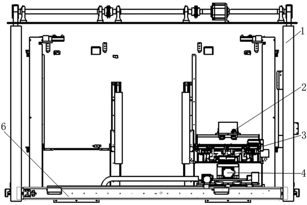
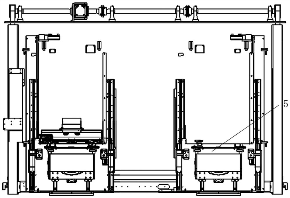
[0033] see figure 1 , Picture 1-1 , a device structure for picking and placing large-scale semiconductor printed boards of the present invention, including a Z-direction moving structure 1, a camera structure 2, a Y-direction moving structure 3, a U-direction rotating structure 4, a loading platform structure 5, and an X-direction moving structure 6;

[0034] The loading platform structure 5 is used to realize the lifting of the loading platform 57;

[0035...


PUM


Abstract

The invention discloses an equipment structure for taking and placing a large semiconductor printing plate. The equipment structure comprises a Z-direction moving structure, a camera structure, a Y-direction moving structure, a U-direction rotating structure, a feeding platform structure and an X-direction moving structure; the feeding platform structure is used for achieving lifting of the feeding platform; the X-direction moving structure is used for realizing X-direction movement of a transfer platform; the Y-direction moving structure is used for realizing Y-direction movement of the transfer platform; the Z-direction moving structure is used for realizing Z-direction movement of the transfer platform; the U-direction rotating structure rotates by the rotating platform; and the camerastructure comprises a camera and a light source below the camera. A conductor printing plate taking and placing device is provided with the Z-direction moving structure, the camera structure, the Y-direction moving structure, the U-direction rotating structure, the feeding platform structure and the X-direction moving structure, movement of the transfer platform in the X direction, the Y direction, the Z direction and the U direction is achieved, moving and grabbing are conducted according to the positions of all material pieces in a material box, and automatic taking and placing of a printingplate are achieved; and the production efficiency is improved, and mistaken damage possibly caused by manual taking and placing is avoided.

Description

technical field [0001] The invention relates to a pick-and-place equipment, in particular to a pick-and-place equipment structure for a large semiconductor printed board. Background technique [0002] In the production process of semiconductors, part of the process involves the pick-and-place of large printed boards, that is, taking out or storing them from bins. If these tasks are completed manually, the efficiency is very low, and the labor cost and time cost are relatively high. Therefore, the present invention provides a mechanical structure that can be automatically stored. Contents of the invention [0003] In order to solve the above-mentioned technical problems, the present invention provides a device structure for picking and placing large-scale semiconductor printed boards, which can be automatically picked and stored. [0004] The present invention provides following technical scheme: [0005] A device structure for picking and placing large-scale semiconducto...

Claims


Application Information

Patent Timeline
IPC IPC(8): B65G49/07
CPCB65G49/07
Inventor 赵凯林海涛卢升倪海铨梁猛
Owner 技感半导体设备(南通)有限公司
Why Eureka
Try Eureka