Chip package structure

A chip packaging structure and chip technology, applied in the direction of semiconductor/solid-state device components, semiconductor devices, electrical components, etc., can solve the problems of increased power consumption, high thickness of the packaging structure, and increased resistance, so as to reduce the resistance value, reduce The effect of the overall width

Pending Publication Date: 2021-07-16
POWERTECH TECHNOLOGY INC
View PDF0 Cites 0 Cited by
  • Summary
  • Abstract
  • Description
  • Claims
  • Application Information

AI Technical Summary

Problems solved by technology

However, there are still disadvantages in the way of stacking chips. For example, stacking chips vertically will cause the thickness of the package structure to be too high, and the resistance of the chip stacked on the top to be electrically connected to the circuit board will become larger, which will increase power consumption.

Method used


Image

  • Chip package structure
  • Chip package structure
  • Chip package structure

Examples


Embodiment Construction

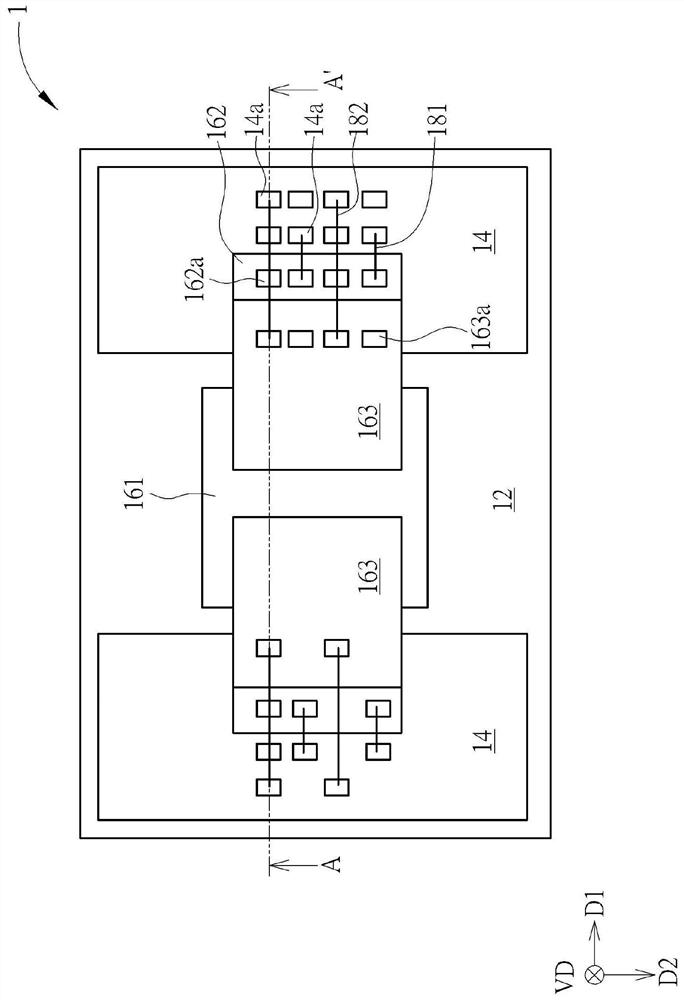
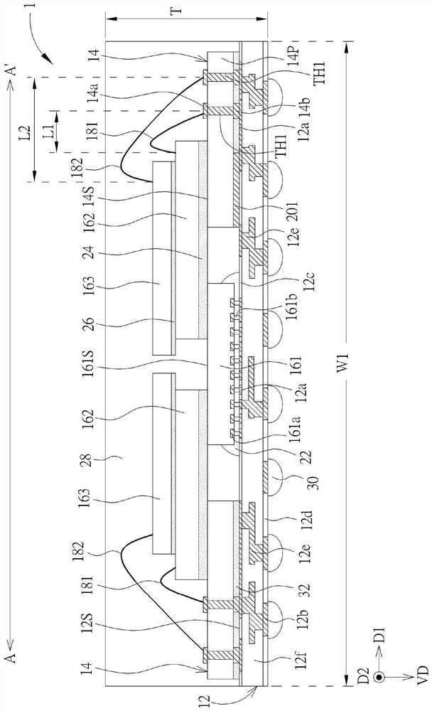
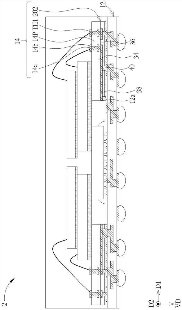
[0046] The present invention can be understood by referring to the following detailed description in conjunction with the drawings. It should be noted that, in order to make the readers easy to understand and the drawings are concise, the drawings of the present invention only draw at least a part of the chip package structure, and the drawings Certain elements in the formulas are not drawn to actual scale. In addition, the quantity and size of each element in the drawings are only for illustration, and are not intended to limit the scope of the present invention.

[0047] Throughout the specification and scope of the appended claims, certain terms will be used to refer to particular elements. Those skilled in the art should understand that electronic device manufacturers may refer to the same element by different names. This document does not intend to distinguish between those elements that have the same function but have different names. In the description and claims belo...


PUM


Abstract

The invention provides a chip package structure including a circuit board, a first die, a spacer, and a second die. The first die is disposed on the circuit board, and the spacer is disposed on the circuit board, in which the spacer includes a spacer part and at least one via structure penetrating through the spacer part. The second die is disposed on the first die and the spacer, and the second die is electrically connected to the circuit board through the spacer.

Description

technical field [0001] The present invention relates to a chip packaging structure, in particular to a chip packaging structure with multi-chip stacking. Background technique [0002] With the miniaturization and multi-functionalization of electronic products, multi-chip packaging structures are becoming more and more common in many electronic products. It is to package two or more chips in a single package structure to reduce the overall volume. In a common multi-chip packaging structure, more than two chips are arranged side by side on the same substrate, but the side-by-side arrangement of the chips will increase the area of ​​the packaging structure as the number of chips increases. To solve this problem, a stacking method is currently developed to configure chips. However, there are still disadvantages in the way of stacking chips, for example, stacking chips vertically will cause the package structure to be too thick, and the resistance of the chip stacked on the top ...

Claims


Application Information

Patent Timeline
Patent Type & Authority Applications(China)
IPC IPC(8): H01L25/18H01L25/065H01L23/498
CPCH01L25/18H01L25/0655H01L23/49811H01L23/49827H01L23/49838H01L25/0652H01L25/0657H01L24/42H01L2225/0651H01L2225/06506H01L2225/06562H01L23/49816H01L23/5385H01L23/5384H01L2224/83191H01L2224/32145H01L2224/49175H01L2224/8592H01L2224/48091H01L2224/16225H01L2224/73265H01L2924/181H01L2224/48227H01L2924/15311H01L2224/73253H01L2924/15184H01L2924/00014H01L2224/32225H01L2224/73204H01L2224/8314H01L24/32H01L24/83H01L2924/1433H01L24/73H01L24/85H01L24/48H01L24/16H01L24/81H01L2924/1434H01L2924/19107H01L2224/05553H01L24/05H01L2224/04042H01L2924/00012H01L2224/45099H01L23/12
Inventor 苏志彦林俊德
Owner POWERTECH TECHNOLOGY INC
Why Eureka
Try Eureka