Perovskite/silicon laminated solar cell and preparation method thereof

A solar cell and perovskite technology, applied in the field of solar cells, can solve the problems of inability to achieve simultaneous passivation of multiple types of defects and low efficiency of carrier interface suppression.

Inactive Publication Date: 2021-07-30
UNIV OF ELECTRONICS SCI & TECH OF CHINA
View PDF8 Cites 11 Cited by
  • Summary
  • Abstract
  • Description
  • Claims
  • Application Information

AI Technical Summary

Problems solved by technology

[0006] The purpose of the present invention is to solve the problems that the interfacial passivation of perovskite materials in the existing perovskite / silicon tandem solar cells cannot achieve simultaneous passivation of multiple types of defects, and the suppression efficiency of carrier interface recombination is not high. Novel perovskite / silicon tandem solar cell and preparation method thereof; in the novel perovskite / silicon tandem solar cell, an organic ionic modifier is provided at the interface of the perovskite light-absorbing layer and the hole transport layer. layer, realize the synchronous and efficient passivation of multiple types of defects at the interface of the perovskite light-absorbing layer, and then effectively improve the photoelectric performance of the perovskite / silicon tandem solar cell

Method used


Image

  • Perovskite/silicon laminated solar cell and preparation method thereof
  • Perovskite/silicon laminated solar cell and preparation method thereof
  • Perovskite/silicon laminated solar cell and preparation method thereof

Examples


Embodiment Construction

[0033] The following describes the preferred embodiments of the present invention with reference to the accompanying drawings to make the technical content clearer and easier to understand. The present invention can be embodied in many different forms of embodiments, and the protection scope of the present invention is not limited to the embodiments mentioned herein.

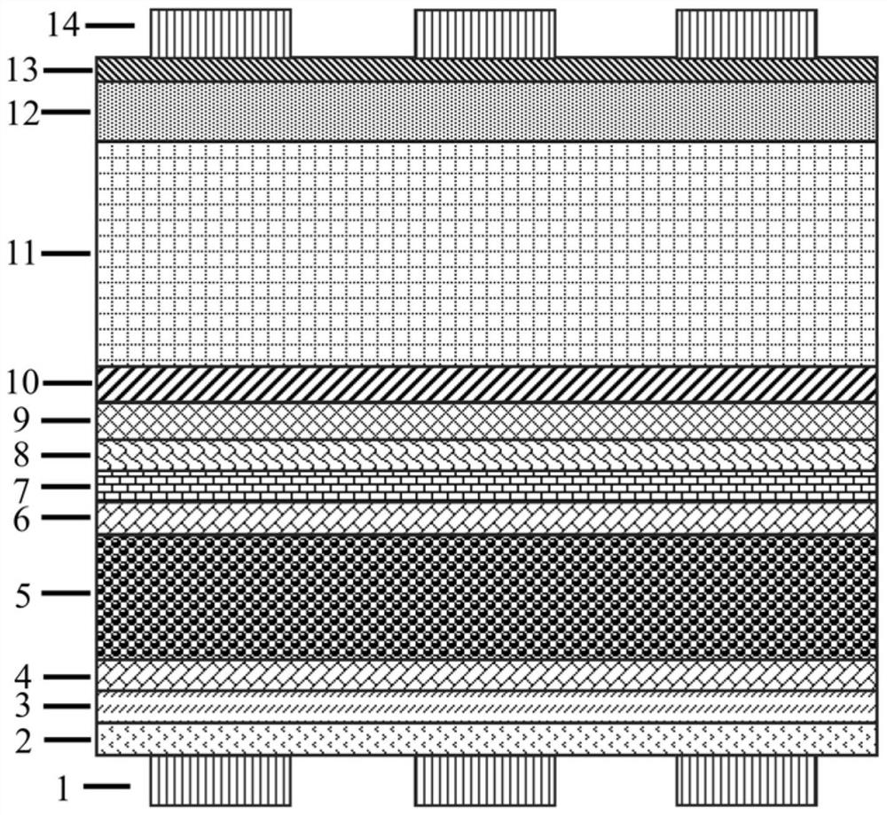
[0034] This embodiment provides a perovskite / silicon stacked solar cell based on the passivation of organic ionic modifiers, the structure of which is as follows figure 1 As shown, it includes: back conductive gate line 1, first ITO transparent conductive layer 2, n-type amorphous silicon layer 3, i-type amorphous silicon layer 4, crystalline silicon layer 5, i-type amorphous silicon layer stacked sequentially from bottom to top. Crystalline silicon layer 6, p-type amorphous silicon layer 7, second ITO transparent conductive layer 8, hole transport layer 9, organic ion modifier passivation layer 10, perovskite li...


PUM


Abstract

The invention belongs to the technical field of solar cells, provides a perovskite / silicon laminated solar cell and a preparation method thereof, and aims to solve the problems that synchronous passivation of multiple types of defects cannot be realized by perovskite material interface passivation in the prior art, the suppression efficiency of carrier interface recombination is low and the like. An organic ionic modifier passivation layer is introduced between a perovskite light absorption layer and a hole transport layer of the perovskite / silicon laminated cell, so that synchronous and efficient passivation of multiple types of defects of an interface is realized, and the defect state density is remarkably reduced; and meanwhile, lattice mismatch at the interface is effectively prevented, and the defect passivation effect is further optimized. In conclusion, the perovskite / silicon laminated solar cell has lower defect state density and higher short-circuit current density and open-circuit voltage, and the overall performance of the perovskite / silicon laminated solar cell is remarkably improved; and moreover, the organic ionic modifier passivation layer is mature in synthesis process and low in price, and has the advantages of high efficiency, stability and low cost.

Description

technical field [0001] The invention belongs to the technical field of solar cells, and specifically provides a perovskite / silicon stacked solar cell and a preparation method thereof. Background technique [0002] In the 21st century, facing severe energy shortages, environmental pollution and other problems, the development and utilization of clean and renewable energy is an urgent task for our country; solar energy has become one of the new energy sources that has attracted much attention due to its green environmental protection, low price and abundant reserves. , is considered to be one of the most promising alternatives to replace traditional fossil fuels. As an important way to effectively utilize solar energy, the development of solar cells has received increasing attention, and among many photovoltaic devices, Perovskite Solar Cells (PSCs) have developed rapidly in recent years. [0003] Perovskite (CH 3 NH 3 PB 3 ) solar cells belong to the third generation of s...

Claims


Application Information

Patent Timeline
Patent Type & Authority Applications(China)
IPC IPC(8): H01L27/30H01L51/46H01L51/48H01L51/44B82Y10/00B82Y40/00
CPCB82Y10/00B82Y40/00H10K30/57H10K19/20H10K85/60H10K85/654H10K30/88Y02E10/549
Inventor 刘明侦崔翔胡逾超李发明
Owner UNIV OF ELECTRONICS SCI & TECH OF CHINA
Why Eureka
Try Eureka