Supercharge Your Innovation With Domain-Expert AI Agents!

Method and system for controlling light erasing voltage of liquid crystal writing device

A technology for erasing voltage and writing devices, which is applied in optics, nonlinear optics, instruments, etc., can solve the problems of slow voltage change between the base layer and liquid crystal layer, long erasing time, and poor TFT photosensitivity, so as to improve writing Experience, improve writing efficiency, and avoid the effect of fading handwriting

Active Publication Date: 2021-11-23
SHANDONG LANBEISITE EDUCATIONAL EQUIP GRP
View PDF13 Cites 0 Cited by
  • Summary
  • Abstract
  • Description
  • Claims
  • Application Information

AI Technical Summary

Problems solved by technology

[0004] In the above scheme, each TFT position on the base layer is correspondingly provided with a TFT light-transmitting port for receiving light irradiation; figure 1 The relationship curve between the illumination time and the voltage difference between the base layer and the liquid crystal layer, if the TFT light-transmitting opening is small, the luminous flux that shines on the TFT through the opening is small, and the light conduction current is small, and the base layer The voltage change between the liquid crystal layer and the liquid crystal layer is slow, and it takes a long time to illuminate to make the voltage difference between the set erasing electrode and the conductive layer reach the erasing voltage of the liquid crystal, resulting in a longer erasing time and lower writing Erase efficiency, poor user experience
[0005] On the other hand, affected by the doping concentration of the TFT channel, if the doping concentration of the TFT channel is small, the photosensitivity of the TFT will deteriorate, which will also make the photoconduction current too small, thereby affecting the time required for partial erasing.
[0006] When the storage capacitor design on the TFT substrate is large, the voltage changes slowly and the erasing time is very long

Method used


Image

  • Method and system for controlling light erasing voltage of liquid crystal writing device
  • Method and system for controlling light erasing voltage of liquid crystal writing device
  • Method and system for controlling light erasing voltage of liquid crystal writing device

Examples


Embodiment 1

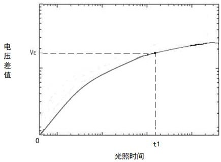
[0032] As described in the background technology, when light is used for partial erasing, the photoconductive current will be too small due to the small TFT light transmission port, too low doping concentration of the TFT channel, or too large storage capacitance, resulting in The charging voltage between the base layer and the liquid crystal layer is small, and it takes a long time to illuminate to make the voltage difference between the set erasing electrode and the conductive layer reach the erasing voltage of the liquid crystal, and the time required for partial erasing Longer, lower writing and erasing efficiency, poor user experience.

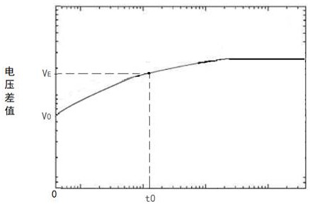
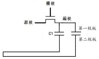
[0033] According to an embodiment of the present invention, a method for controlling an illumination erasing voltage of a liquid crystal writing device is disclosed. The liquid crystal writing device based on the method includes: a conductive layer, a bistable liquid crystal layer, and a base layer arranged sequentially from top to bottom....

Embodiment 2

[0057] According to an embodiment of the present invention, an embodiment of an illumination erasing voltage control system for a liquid crystal writing device is disclosed, which specifically includes:

[0058] A voltage control module, used to control the voltage difference between the base layer and the conductive layer within a set voltage value range below the erasing voltage of the liquid crystal;

[0059] The partial erasing module is used to control all or a set part of TFTs on the base layer to be in a critical state, and realize partial erasing by using light irradiation within a set intensity range.

[0060] It should be noted that the specific implementation manners of the above modules have been described in detail in Embodiment 1, and will not be described in detail here.

Embodiment 3

[0062] According to an embodiment of the present invention, a voltage drive controller is disclosed, and the controller loads and executes the method for controlling the illumination erasing voltage of a liquid crystal writing device described in Embodiment 1.


PUM


Abstract

The invention discloses a method and system for controlling the erasing voltage of a liquid crystal writing device, comprising: controlling the voltage difference between the base layer and the conductive layer within a set voltage range lower than the erasing voltage of the liquid crystal; and then controlling All or a set part of the TFTs on the base layer are in a critical state, and partial erasing is realized by irradiating light within a set intensity range. The present invention shortens the time required for the light conduction of the TFT by pre-loading the voltage between the base layer and the liquid crystal layer, thereby increasing the local erasing speed.

Description

technical field [0001] The invention relates to the technical field of liquid crystal writing boards, in particular to a method and system for controlling light erasing voltage of a liquid crystal writing device. Background technique [0002] The working principle of the liquid crystal writing board currently on the market is to use the bistable property of the liquid crystal to display and / or erase the written content on the liquid crystal writing board. Taking cholesteric liquid crystal as an example, the writing pressure track of the writing pen is recorded by changing the liquid crystal state at the tip of the pen by the pressure acting on the liquid crystal writing board, and then the corresponding writing content is displayed; the structure of the cholesteric liquid crystal is changed by applying an electric field, Thereby, the writing track on the liquid crystal writing board disappears to realize erasing. [0003] Patent No. CN112684618B discloses a technical soluti...

Claims


Application Information

Patent Timeline
Patent Type & Authority Patents(China)
IPC IPC(8): G02F1/133
CPCG02F1/13306
Inventor 李清波杨猛训
Owner SHANDONG LANBEISITE EDUCATIONAL EQUIP GRP
Features
  • R&D
  • Intellectual Property
  • Life Sciences
  • Materials
  • Tech Scout
  • Unparalleled Data Quality
  • Higher Quality Content
  • 60% Fewer Hallucinations
Learn More