Touch sensor panel
A touch sensor and touch window technology, applied in instruments, computing, electrical and digital data processing, etc., can solve problems such as device malfunction, wrong judgment, touch signal change, etc., to improve upper and lower split, prevent upper and lower split, and avoid misoperation Effect
- Summary
- Abstract
- Description
- Claims
- Application Information
AI Technical Summary
Problems solved by technology
Method used
Image

Examples
no. 1 approach
[0081] Figure 8a is an enlarged schematic diagram of a part of the arrangement structure of the driving electrodes and the receiving electrodes of the touch sensor panel according to the first embodiment, Figure 8b is a conductive bar contact showing 15(phi) Figure 8a The left-right split is shown in the case of the touch sensor board in the floating state to improve the experimental data.
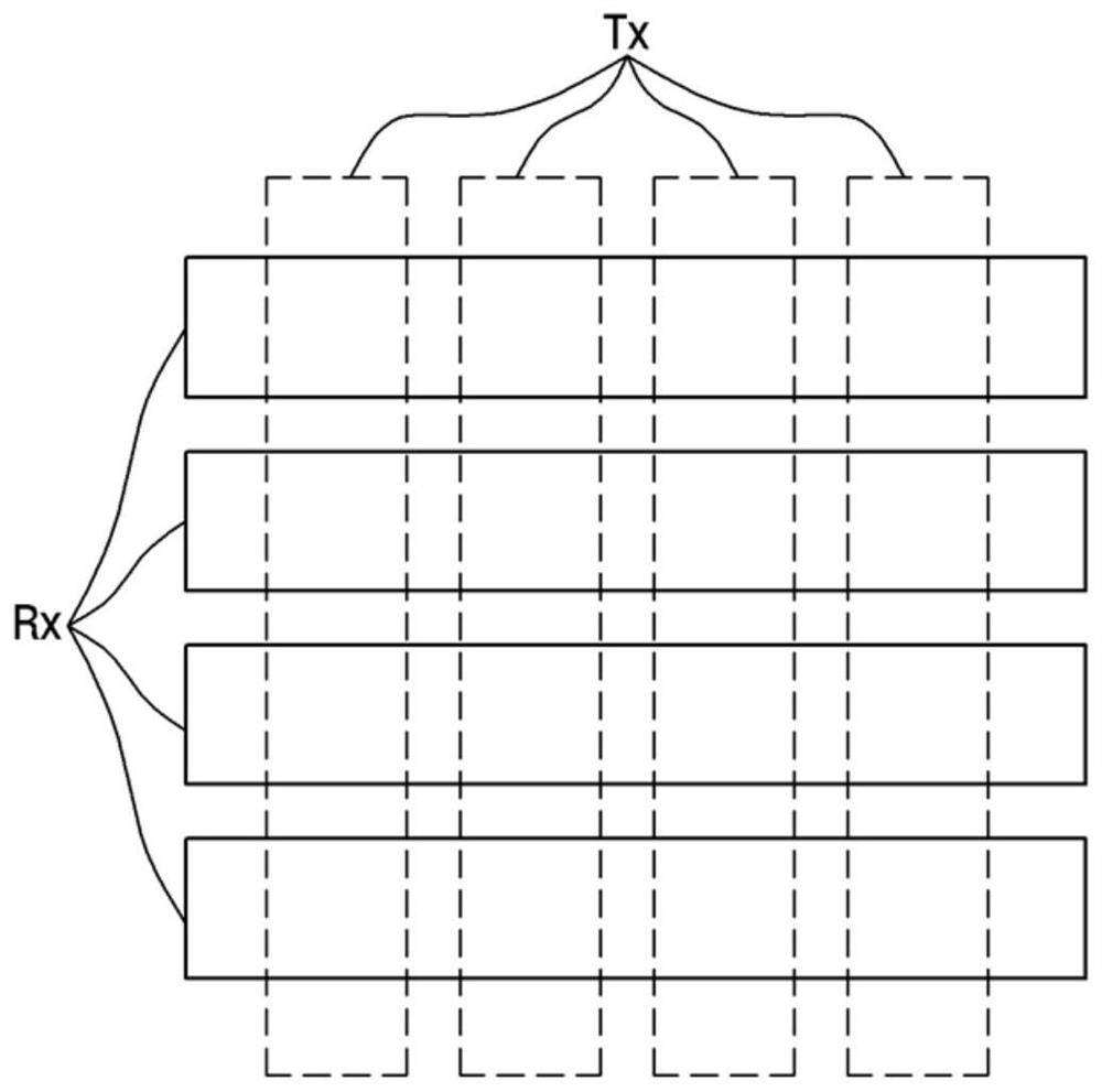
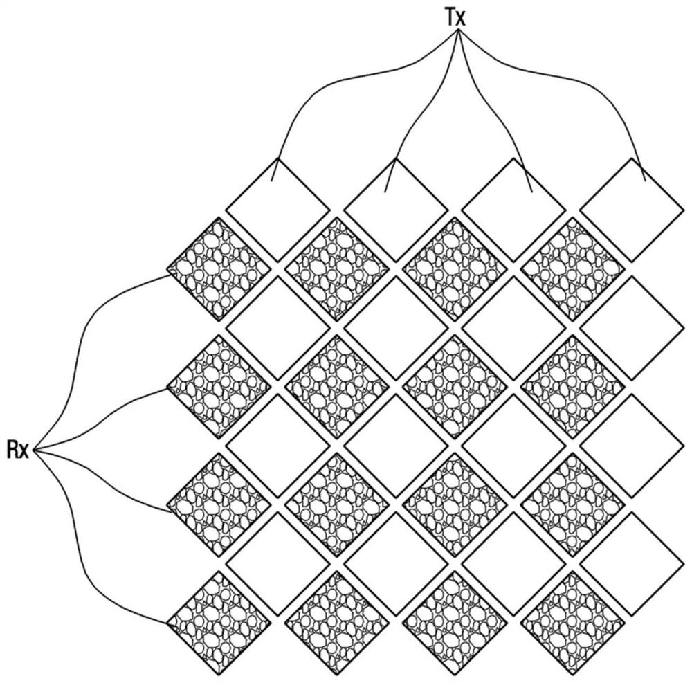
[0082] see Figure 8a , the touch sensor board of the first embodiment includes a plurality of driving electrodes TX and a plurality of receiving electrodes RX. A plurality of driving electrodes TX and a plurality of receiving electrodes RX are arranged in a matrix on the same layer.
[0083] The plurality of driving electrodes TX and the plurality of receiving electrodes RX can be made of transparent conductive material (for example, indium tin oxide (ITO: Indium Tin Oxide) or antimony tin oxide (SnO2) composed of tin oxide (SnO2) and indium oxide (In2O3) ATO: Antimony Tin Oxide)) ...
no. 2 approach
[0096] Figure 9a is an enlarged schematic diagram of a part of the arrangement structure of the driving electrodes and the receiving electrodes of the touch sensor panel according to the second embodiment, Figure 9b is a conductive bar contact showing 15(phi) Figure 9a The left-right split is shown in the case of the touch sensor board in the floating state to improve the experimental data.
[0097] see Figure 9a , the touch sensor board of the second embodiment includes a plurality of driving electrodes TX and a plurality of receiving electrodes RX. A plurality of driving electrodes TX and a plurality of receiving electrodes RX are arranged in a matrix on the same layer.
[0098] The plurality of driving electrodes TX and the plurality of receiving electrodes RX can be made of transparent conductive material (for example, indium tin oxide (ITO: Indium Tin Oxide) or antimony tin oxide (SnO2) composed of tin oxide (SnO2) and indium oxide (In2O3) ATO: Antimony Tin Oxide)...
no. 3 approach
[0110] Figure 10a is an enlarged schematic diagram of a part of the arrangement structure of the driving electrodes and the receiving electrodes of the touch sensor panel according to the third embodiment, Figure 10b is the conductive rod showing 15(phi) at Figure 10a Shown is experimental data showing improved left-right splitting when touch is made with the touch sensor board in a floating state.
[0111] see Figure 10a , The touch sensor board of the third embodiment includes a plurality of driving electrodes TX and a plurality of receiving electrodes RX. A plurality of driving electrodes TX and a plurality of receiving electrodes RX are arranged in a matrix on the same layer.
[0112] The plurality of driving electrodes TX and the plurality of receiving electrodes RX can be made of transparent conductive material (for example, indium tin oxide (ITO: Indium Tin Oxide) or antimony tin oxide (SnO2) composed of tin oxide (SnO2) and indium oxide (In2O3) ATO: Antimony Ti...
PUM
| Property | Measurement | Unit |
|---|---|---|
| length | aaaaa | aaaaa |
Abstract
Description
Claims
Application Information
 - R&D Engineer
- R&D Manager
- IP Professional
- Industry Leading Data Capabilities
- Powerful AI technology
- Patent DNA Extraction
Browse by: Latest US Patents, China's latest patents, Technical Efficacy Thesaurus, Application Domain, Technology Topic.
© 2024 PatSnap. All rights reserved.Legal|Privacy policy|Modern Slavery Act Transparency Statement|Sitemap