Shift register circuit and image display apparatus containing the same

A shift register, circuit technology, used in logic circuits, static memory, digital memory information and other directions

Inactive Publication Date: 2008-09-10
MITSUBISHI ELECTRIC CORP
View PDF3 Cites 95 Cited by
  • Summary
  • Abstract
  • Description
  • Claims
  • Application Information

AI Technical Summary

Problems solved by technology

[0024] As described above, although Patent Document 2's Figure 7 The unit shift register has a transistor T1A to prevent the above problems, but since its gate fluctuates according to the clock signal, it is turned off at the cycle of the clock signal
Therefore, when the off-state current of the transistors T0 and T1 is large, the level of the gate may exceed the threshold voltage while the transistor T1A is off.

Method used


Image

  • Shift register circuit and image display apparatus containing the same
  • Shift register circuit and image display apparatus containing the same
  • Shift register circuit and image display apparatus containing the same

Examples


Embodiment approach 1

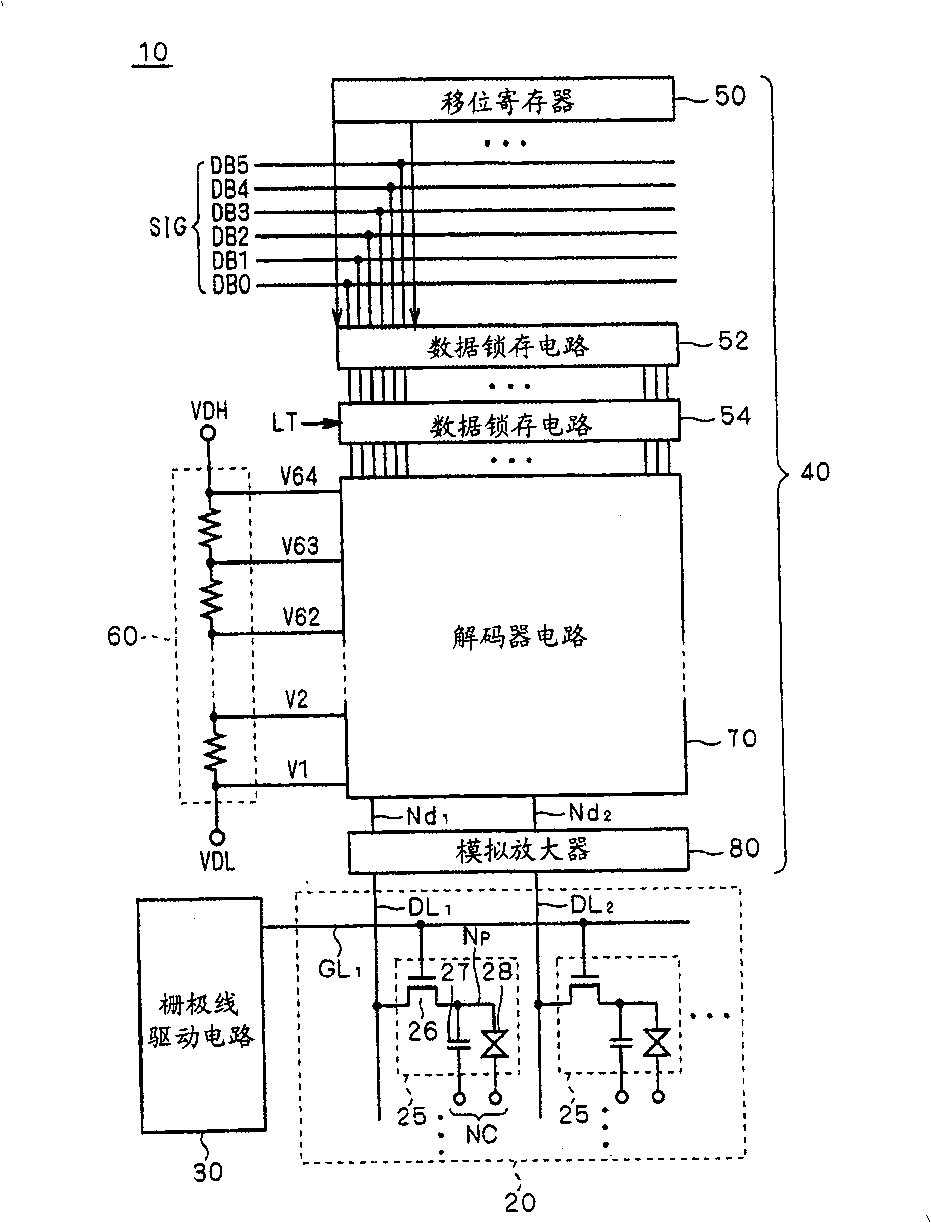
[0070] figure 1 It is a schematic block diagram showing the configuration of the display device according to Embodiment 1 of the present invention, and shows the overall configuration of a liquid crystal display device 10 as a representative example of the display device.

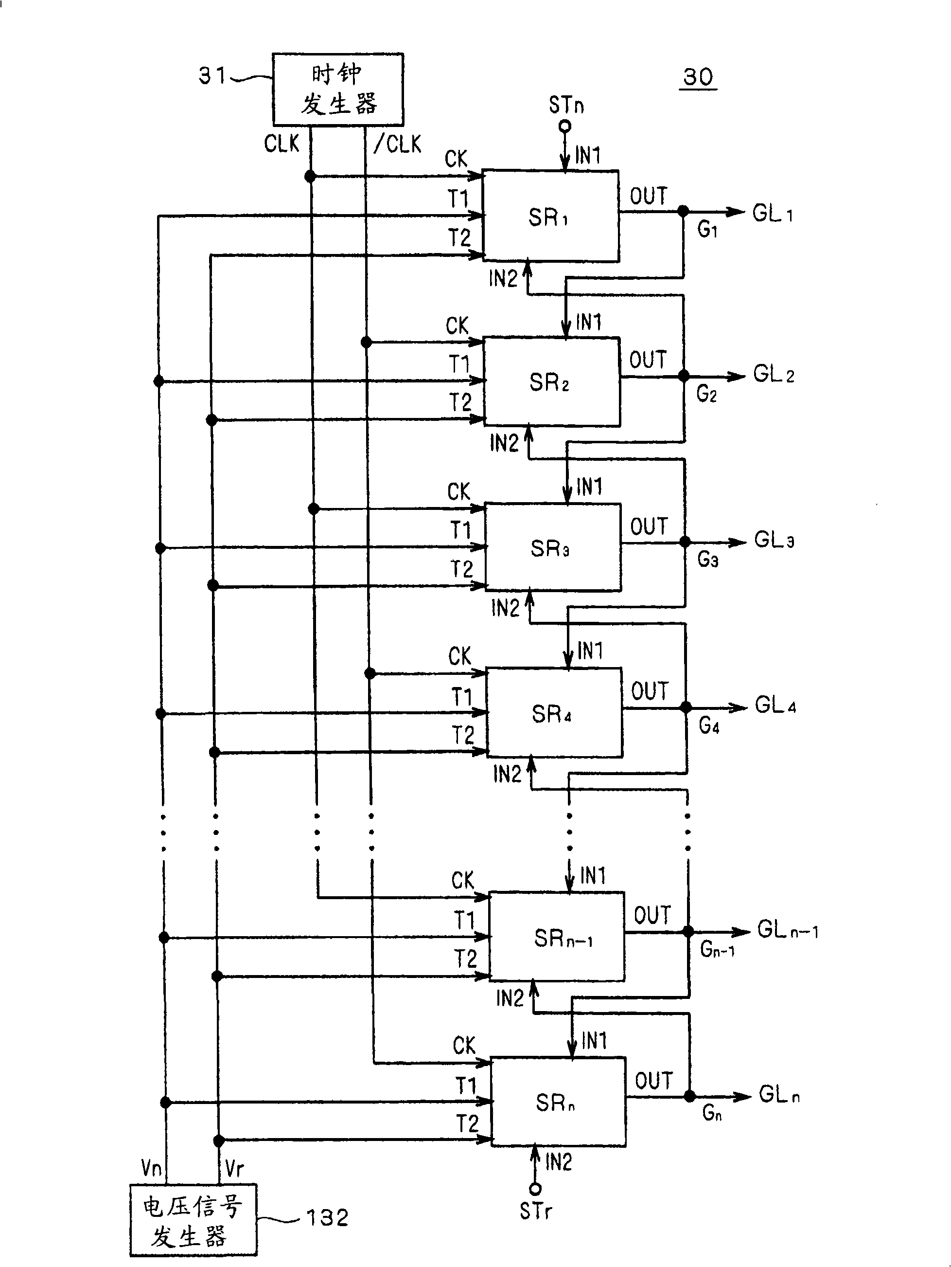
[0071] The liquid crystal display device 10 includes a liquid crystal array unit 20 , a gate line driver circuit (scanning line driver circuit) 30 , and a source driver 40 . As will be apparent from the description below, the bidirectional shift register according to the embodiment of the present invention is mounted on the gate line driver circuit 30 and integrally formed with the liquid crystal array unit 20 .

[0072] The liquid crystal array unit 20 includes a plurality of pixels 25 arranged in a matrix. Gate lines GL are respectively provided in rows of pixels (hereinafter also referred to as "pixel rows") 1 、GL 2 ... (collectively referred to as "gate lines GL"), and in addition, data lines DL are...

Embodiment approach 2

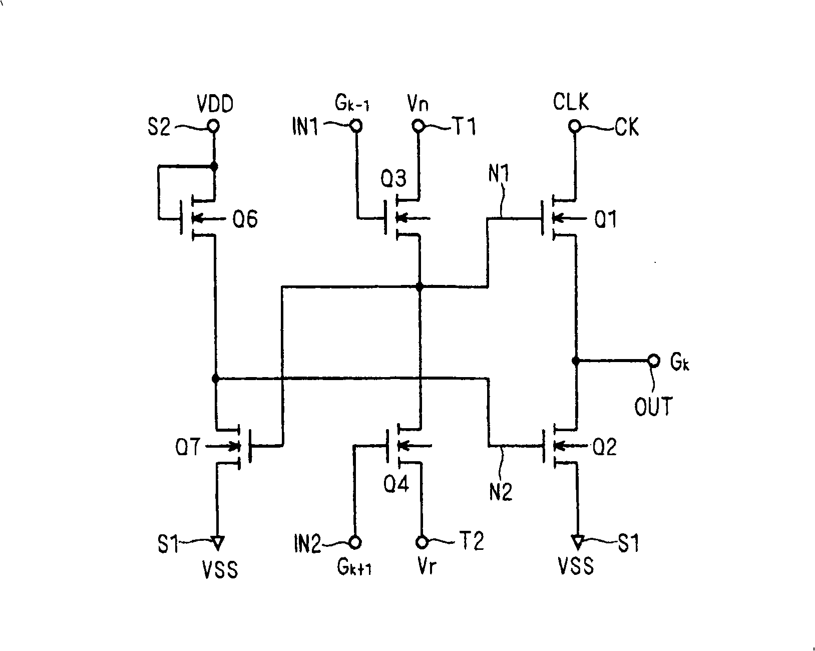
[0172] Here, modified examples of the first pull-down circuit 41 and the second pull-down circuit 42 included in the unit shift register SR of the present invention are shown. However, as described below, regarding the first pull-down circuit 41, since it is basically preferable in Embodiment Mode 1 ( Figure 8 ), therefore, the modification example of the second pull-down circuit 42 will be mainly described below in detail.

[0173] Figure 11 (a) is a circuit diagram of the second pull-down circuit 42 of the second embodiment. exist Figure 11 (a) shows an example in which the clock signal CLK is input to the first clock terminal CK1 and the clock signal / CLK is input to the second clock terminal CK2 (in Figure 12 It is the same in each subsequent circuit diagram).

[0174] In this embodiment, compared to Figure 8 The second pull-down circuit 42 uses transistors Q6B and Q9B instead of the capacitive element C2B. The transistor Q6B is connected between the second cloc...

Embodiment approach 3

[0185] Figure 12 (a) is a circuit diagram of the second pull-down circuit 42 of the third embodiment. In this embodiment, compared to Figure 11 In the circuit of (a), the transistor Q7B is replaced by two transistors Q7Bn and Q7Br. The transistor Q7Bn is connected between the node N4 and the first power supply terminal S1, and its gate is connected to the first input terminal IN1. The transistor Q7Br is connected between the node N4 and the first power supply terminal S1, and its gate is connected to the second input terminal IN2.

[0186] The on-resistance of transistor Q6B is set sufficiently larger than that of transistors Q7Bn and Q7Br, respectively, and the combination of transistors Q6B and Q7Bn and the combination of transistors Q6B and Q7Br constitute a proportional inverter. That is, the on-resistance of the transistors Q7Bn, Q7Br is set sufficiently lower than that of the transistor Q6B. Therefore, in the circuit composed of Q6B, Q7Bn, and Q7Br, assuming that t...


PUM


Abstract

Threshold voltage shifts of transistors which are constituents of a bidirectional shift register are reduced to prevent a malfunction in the shift register. A bidirectional unit shift register includes first and second pull-down circuits (41, 42) connected to the gate of a first transistor (Q1) that supplies a first clock signal (CLK) to an output terminal (OUT). The first pull-down circuit (41) includes a first inverter that uses the gate of the first transistor (Q1) as the input node and that is activated by the first clock signal (CLK), and a second transistor (Q5A) that discharges the gate of the first transistor (Q1) according to the output of the first inverter. The second pull-down circuit (42) includes a second inverter that uses the gate of the first transistor (Q1) as the input node and that is activated by a second clock signal ( / CLK) having a different phase from the first clock signal (CLK), and a third transistor (Q5A) that discharges the gate of the first transistor according to the output of the second inverter.

Description

technical field [0001] The present invention relates to a shift register circuit composed only of field effect transistors of the same conductivity type used in, for example, scanning line driving circuits of image display devices, and more particularly to a bidirectional shift register capable of reversing the direction of signal shifting. Background technique [0002] In an image display device such as a liquid crystal display device (hereinafter referred to as a "display device"), a gate line (scanning line) is provided for each pixel row (pixel line) of a display panel arranged in a matrix of pixels to display a signal. A period of one horizontal period selects and drives the gate line sequentially, so as to update the display image. Thus, as a gate line driver circuit (scanning line driver circuit) for sequentially selecting and driving pixel lines, that is, gate lines, a shift register that performs a round-trip shift operation during one frame period of a display sign...

Claims


Application Information

Patent Timeline
Patent Type & Authority Applications(China)
IPC IPC(8): G11C19/28G11C19/00G09G3/36
CPCH03K19/096G09G3/3677G09G2300/0417G09G2310/0283G09G2310/0286G11C19/184G11C19/28G09G3/20G09G3/36G11C19/00H03K19/00
Inventor 飞田洋一
Owner MITSUBISHI ELECTRIC CORP
Why Eureka
Try Eureka