Method of Forming Gate Insulating Film, Semiconductor Device and Computer Recording Medium

a technology of gate insulation film and semiconductor device, which is applied in the direction of semiconductor devices, instruments, computing, etc., can solve the problems of increasing the film thickness and and achieve the effect of inhibiting the deterioration of the driving capability of the devi

Inactive Publication Date: 2007-12-20
TOKYO ELECTRON LTD
View PDF5 Cites 7 Cited by
  • Summary
  • Abstract
  • Description
  • Claims
  • Application Information

AI Technical Summary

Benefits of technology

[0013] According to the present invention, a boron penetration phenomenon is prevented in a semiconductor device, yet annealing after plasma nitridation is not necessary, and deterioration in driving capability of the device is inhibited.

Problems solved by technology

However, the above conventional art is an art relating to a MOSFET and requires additional annealing as post-processing.
However, the annealing may possibly increase the film thickness.
In this case, it is also necessary to be careful about nitrogen concentration in the oxide film which is a factor to cause deterioration in driving capability of the device.

Method used


Image

  • Method of Forming Gate Insulating Film, Semiconductor Device and Computer Recording Medium
  • Method of Forming Gate Insulating Film, Semiconductor Device and Computer Recording Medium
  • Method of Forming Gate Insulating Film, Semiconductor Device and Computer Recording Medium

Examples


Embodiment Construction

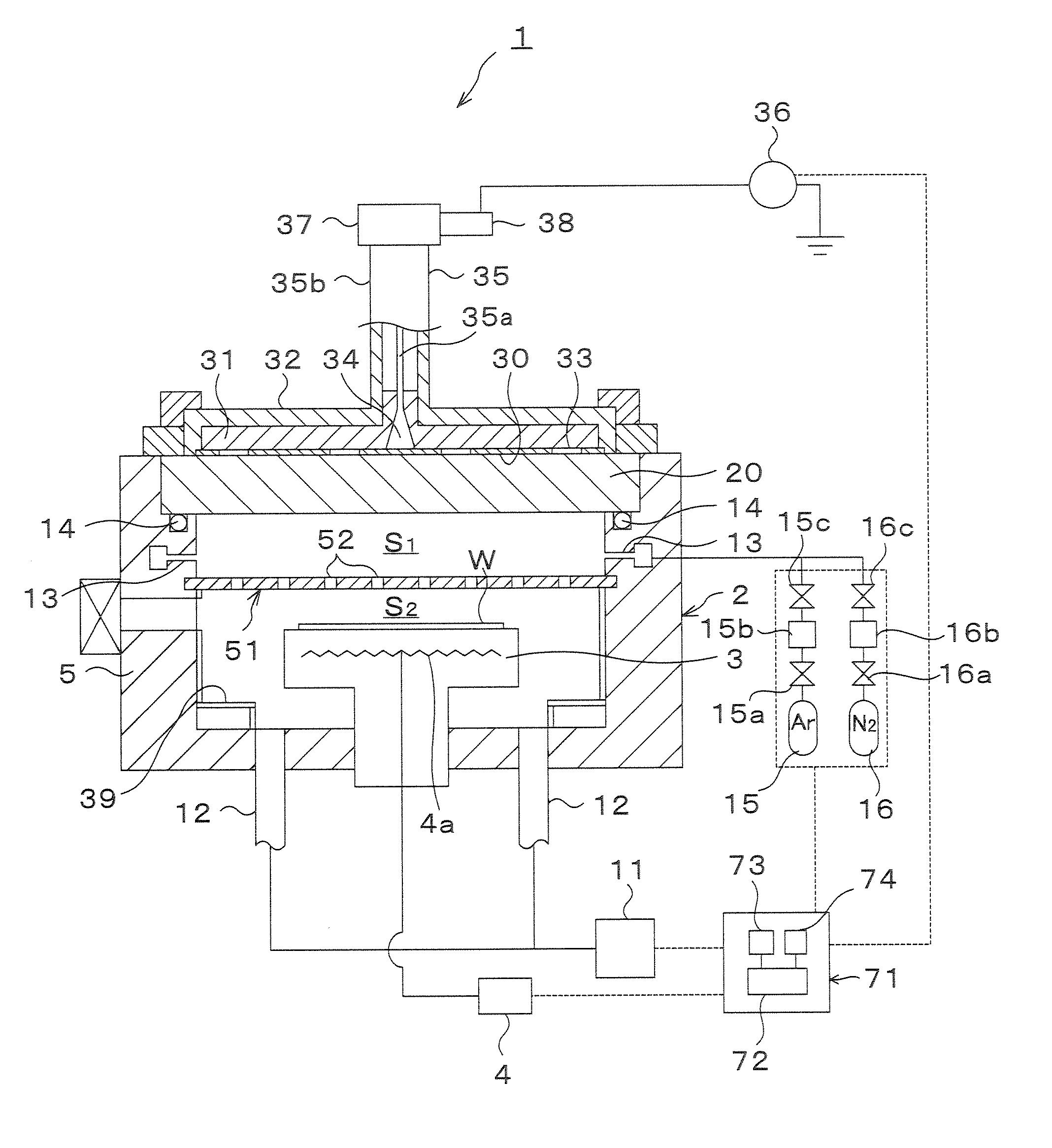
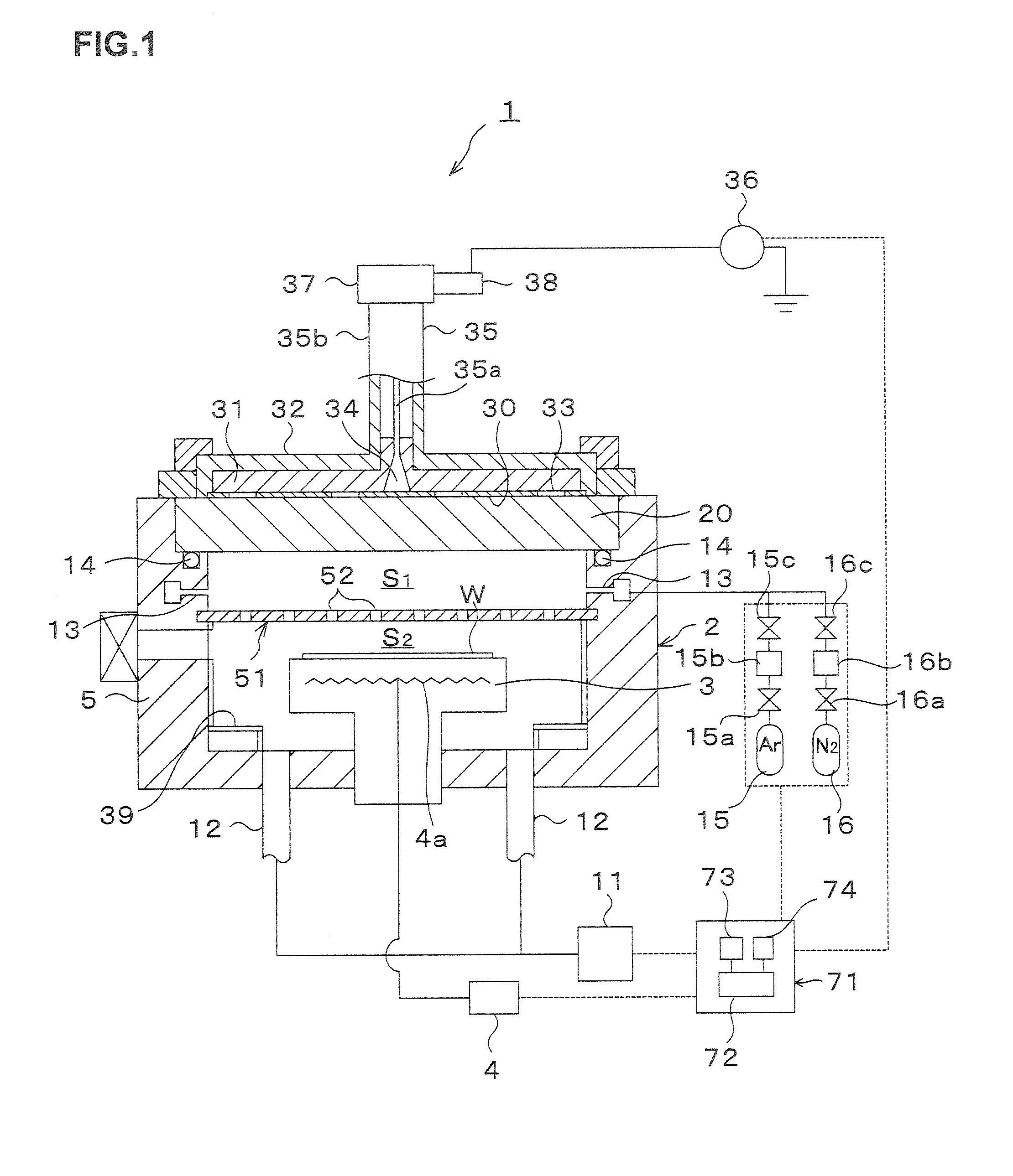
[0037] Hereinafter, an embodiment of the present invention will be described. FIG. 1 shows the appearance of a vertical cross section of a plasma processing apparatus 1 for carrying out a method of forming a gate insulation film according to this embodiment, and this plasma processing apparatus 1 includes a process vessel 2 made of, for example, aluminum and formed in a bottomed cylindrical shape whose upper portion is open. The process vessel 2 is grounded. The process vessel 2 has in a bottom portion thereof a susceptor 3 as a mounting table for placing a substrate, for example, a semiconductor wafer (hereinafter, referred to as a wafer) W thereon. The susceptor 3 is made of, for example, aluminum nitride and has a heater 4a therein. The heater 4a can be constituted of, for example, a resistor, and generates heat when supplied with power from an AC power source 4 provided outside the process vessel 2 and is capable of heating the wafer on the susceptor 3 to a predetermined tempera...


PUM


Abstract

In the present invention, when a gate insulation film in a DRAM is formed, an oxide film constituting a base of the gate insulation film is plasma-nitrided. The plasma nitridation is performed with microwave plasma generated by using a plane antenna having a large number of through holes. Nitrogen concentration in the gate insulation film formed by the plasma nitridation is 5 to 20% in atomic percentage. Even without subsequent annealing, it is possible to effectively prevent a boron penetration phenomenon in the DRAM and to reduce traps in the film causing deterioration in driving capability of the device.

Description

TECHNICAL FIELD [0001] The present invention relates to a method of forming a gate insulation film of a semiconductor device, a semiconductor device, and a computer recording medium. BACKGROUND ART [0002] In a semiconductor device including a silicon oxide film as a gate insulation film, in order to prevent so-called boron penetration which is a phenomenon that boron in a gate electrode penetrates the gate insulation film made of the silicon oxide film to reach a substrate, the silicon oxide film is nitrided with plasma and thereafter is subjected to rapid thermal annealing (Patent document 1). [Patent Document 1] Japanese Patent Application Laid-open No. 2004-48001 [0003] However, the above conventional art is an art relating to a MOSFET and requires additional annealing as post-processing. However, the annealing may possibly increase the film thickness. Therefore, there is a demand for an art which can prevent the boron penetration yet does not require the subsequent annealing ev...

Claims


Application Information

Patent Timeline
Patent Type & Authority Applications(United States)
IPC IPC(8): H01L21/8242H01L27/108
CPCH01L21/28202H01L27/10873H01L21/3145H01L21/3144H10B12/05H01L21/0234H01L21/02332H01L21/67017H01L21/67103H01L21/67248
Inventor NISHITA, TATSUOISHIZUKA, SHUUICHIFUJINO, YUTAKANAKANISHI, TOSHIOSATO, YOSHIHIRO
Owner TOKYO ELECTRON LTD
Why Eureka
Try Eureka