Non-volatile semiconductor memory device for selective cell flash erasing/programming

a non-volatile, memory device technology, applied in static storage, digital storage, instruments, etc., can solve the problems of requiring several tens of seconds, excessive erased state generation depending on memory state, and increased product cos

Inactive Publication Date: 2000-08-29
RENESAS ELECTRONICS CORP
View PDF5 Cites 8 Cited by
  • Summary
  • Abstract
  • Description
  • Claims
  • Application Information

AI Technical Summary

Benefits of technology

In accordance with the non-volatile semiconductor memory device of the present invention, the time length required for the flash programming and the flash erasing can be reduced without the addition of the specific structure thereby reducing the chip area. The memory cell can be selected in accordance with the current drive ability to the memory cell at the time of the flash programming and the flash erasing. and even a power supply circuit having a low current drive ability can be employed.

Problems solved by technology

This inspection requires several tens of seconds, and the cost of the product elevates.
In the non-volatile semiconductor memory device in this gazette, the disadvantage that an excessively erased state is generated depending on the memory state is averted by conducting flash programming before flash erasing at the time of erasing all memory cells (all bits).

Method used


Image

  • Non-volatile semiconductor memory device for selective cell flash erasing/programming
  • Non-volatile semiconductor memory device for selective cell flash erasing/programming
  • Non-volatile semiconductor memory device for selective cell flash erasing/programming

Examples


embodiment 1

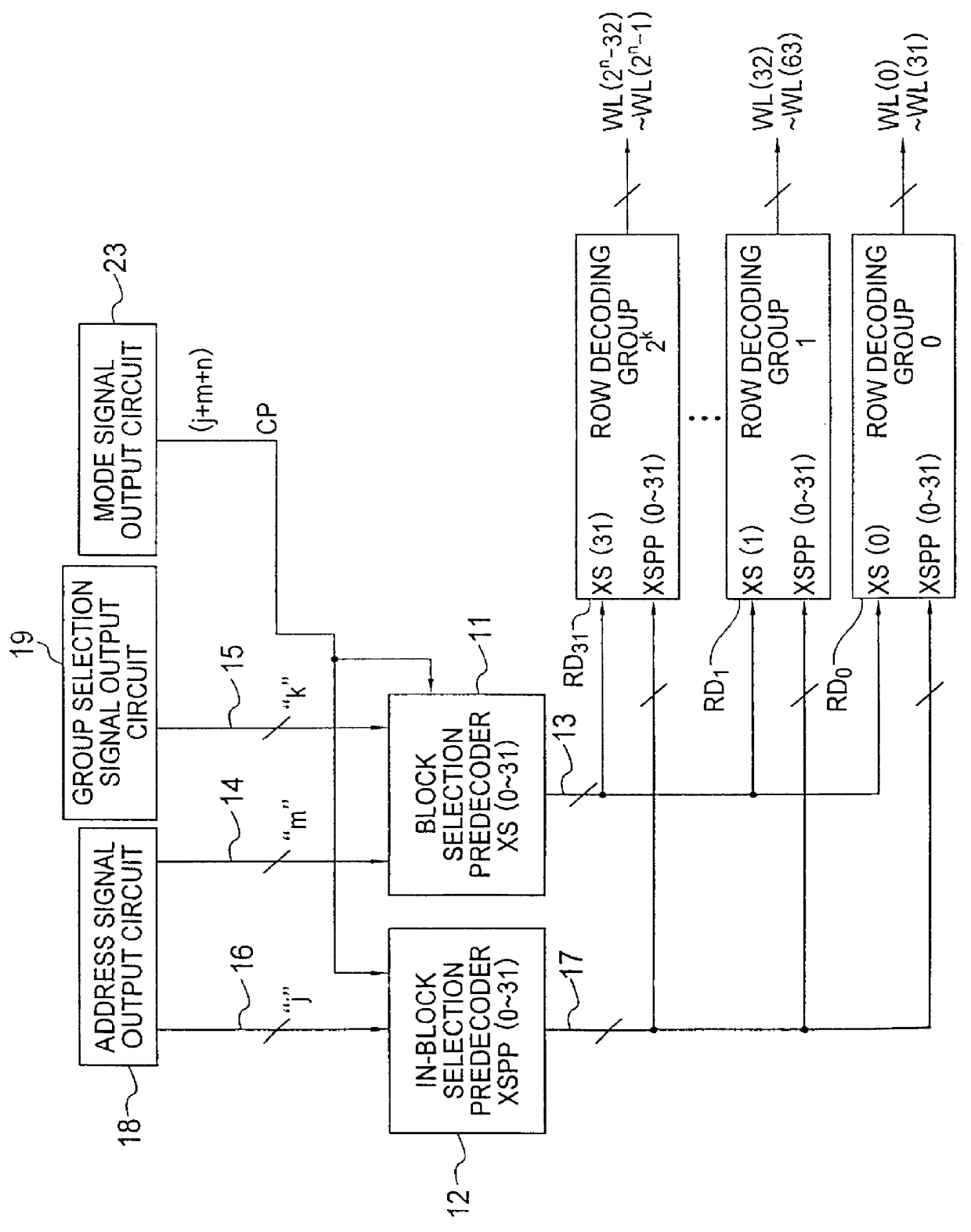
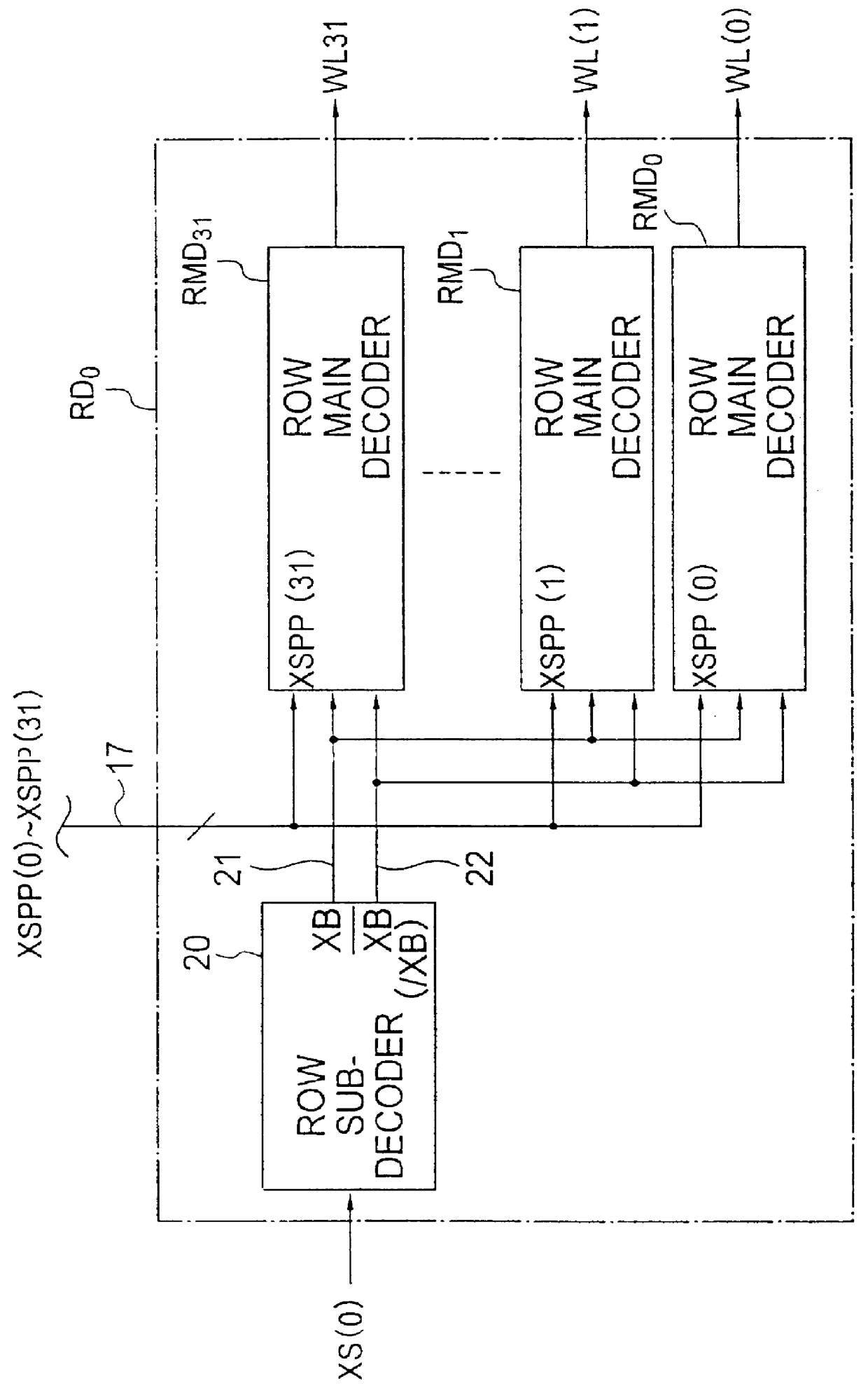
Referring to FIG. 1, a non-volatile semiconductor memory device in accordance an Embodiment of the present invention has a configuration in which the memory cell is divided into 32 memory cell blocks each of which has 32 word lines. A row decoder has a mode signal output circuit 23, a group selection signal output circuit 19, an address signal output circuit 18, a block selection predecoder 11, an in-block selection predecoder 12, and a plurality of row decoding groups RD.sub.0 to RD.sub.31.

The mode signal output circuit 23 has a function of outputting a whole chip selection signal (mode signal) CP for performing the flash programming and the flash erasing of the memory cells.

The group selection signal output circuit 19 is connected to the block selection predecoder 11 through a number "k" of selection signal lines 15, and outputs a word line group selection signal (group selection signal) to the block selection predecoder 11 in timing with the output of the whole chip selection sig...

embodiment 2

FIG. 10 is an equivalent circuit diagram showing a second Embodiment obtained by partly changing the structure of the in-block selection predecoder 12 shown in FIG. 4. An in-block selection predecoder 60 has, similar to the in-block selection predecoder 12, inverters 49,50, OR gates 40 to 43, AND gates 45 to 48 and decoding voltage changing circuits 51 to 54.

In the in-block selection predecoder 60, the OR gate 40 has an input to which a less significant address signal A(0) inverted by the inverter 49 is input, and the OR gate 41 has an input to which a non-inverted less significant address signal A(0) is input. The OR gate 42 has an input to which a less significant address signal A(1) inverted by the inverter 50 is input, and the OR gate 43 has an input to which a non-inverted less significant address signal A(1) is input. Each of the OR gates 40,41 has the other terminal to which a logic product obtained in the AND gate 61 between the whole chip selection signal CP and a checker m...

embodiment 3

FIG. 11 is an equivalent circuit diagram showing a third Embodiment obtained by partly changing the structure of the in-block selection predecoder 12 shown in FIG. 4. An in-block selection predecoder 63 having a word line flash selection function includes, similar to the in-block selection predecoder 12, inverters 49,50, OR gates 40 to 43, AND gates 45 to 48 and decoding voltage changing circuits 51 to 54.

In the in-block selection predecoder 63, the OR gates 40 to 43 are connected between the AND gates 45 to 48 and the decoding voltage changing circuits 51 to 54. In this constitution, the AND gate 45 supplies a logic product between the less significant address signals A(0) and A(1) to one terminal of the OR gate 40, and the AND gate 46 supplies a logic product between the less significant address signal A(0) after its inversion by the inverter 49 and the less significant address signal A(1) to one terminal of the OR gate 41. The AND gate 47 supplies a logic product between the less...


PUM


Abstract

Disclosed herein is a non-volatile semiconductor memory device comprising a mode signal output means for outputting a mode signal for conducting flash programming or flash erasing, a group selection signal output means for outputting a group selection signal for selecting a row decoding group, a first selection means for selecting the row decoding group controlling the word line in accordance with 10 the group selection signal, and a second selection means selecting the word line corresponding to the memory cell from a plurality of the word lines controlled by the row decoding group selected by the first selection means. In the present inventions the time required for the flash programming and the flash erasing can be reduced without the addition of a further element and the chip areas can be reduced.

Description

(a). Field of the InventionThe present invention relates to a non-volatile semiconductor memory device such as flash EEPROM, more in particular to the non-volatile sem-iconductor memory device having a function of selecting a group of word lines.(b). Description of the Related ArtA conventional flash EEPROM includes a memory cell array having a plurality of non-volatile memory cells located at the respective intersections in a matrix formed by a plurality of word lines and a plurality of bit lines. The EEPROM has a row decoder connected to each of the memory cells through a corresponding word line extending in the row direction and a program circuit connected to each of the memory cells through source lines and bit lines both extending perpendicular to the word lines.The memory cell array of the EEPROM may have first and second select transistors, a cell transistor constituting the memory cell and the word lines connected to the respective gates of the first and second select transi...

Claims


Application Information

Patent Timeline
Patent Type & Authority Patents(United States)
IPC IPC(8): G11C16/08G11C8/12G11C8/00G11C16/06G11C16/02
CPCG11C8/12G11C16/08G11C16/06
Inventor OKU, SATORUKOBATAKE, HIROYUKIAMANAI, MASAKAZUKATO, KAZUAKIKANEKO, MASAKI
Owner RENESAS ELECTRONICS CORP
Why Eureka
Try Eureka