Method of designing low power consumption semiconductor integrated circuit

A technology of integrated circuits and design methods, applied in semiconductor/solid-state device manufacturing, circuits, computer-aided design, etc.

Inactive Publication Date: 2004-10-27
PANASONIC CORP
View PDF0 Cites 7 Cited by
  • Summary
  • Abstract
  • Description
  • Claims
  • Application Information

AI Technical Summary

Problems solved by technology

However, no such solution has been found to effectively achieve a rapid reduction in power consumption of a circuit based on final design data.

Method used


Image

  • Method of designing low power consumption semiconductor integrated circuit
  • Method of designing low power consumption semiconductor integrated circuit
  • Method of designing low power consumption semiconductor integrated circuit

Examples


no. 1 example

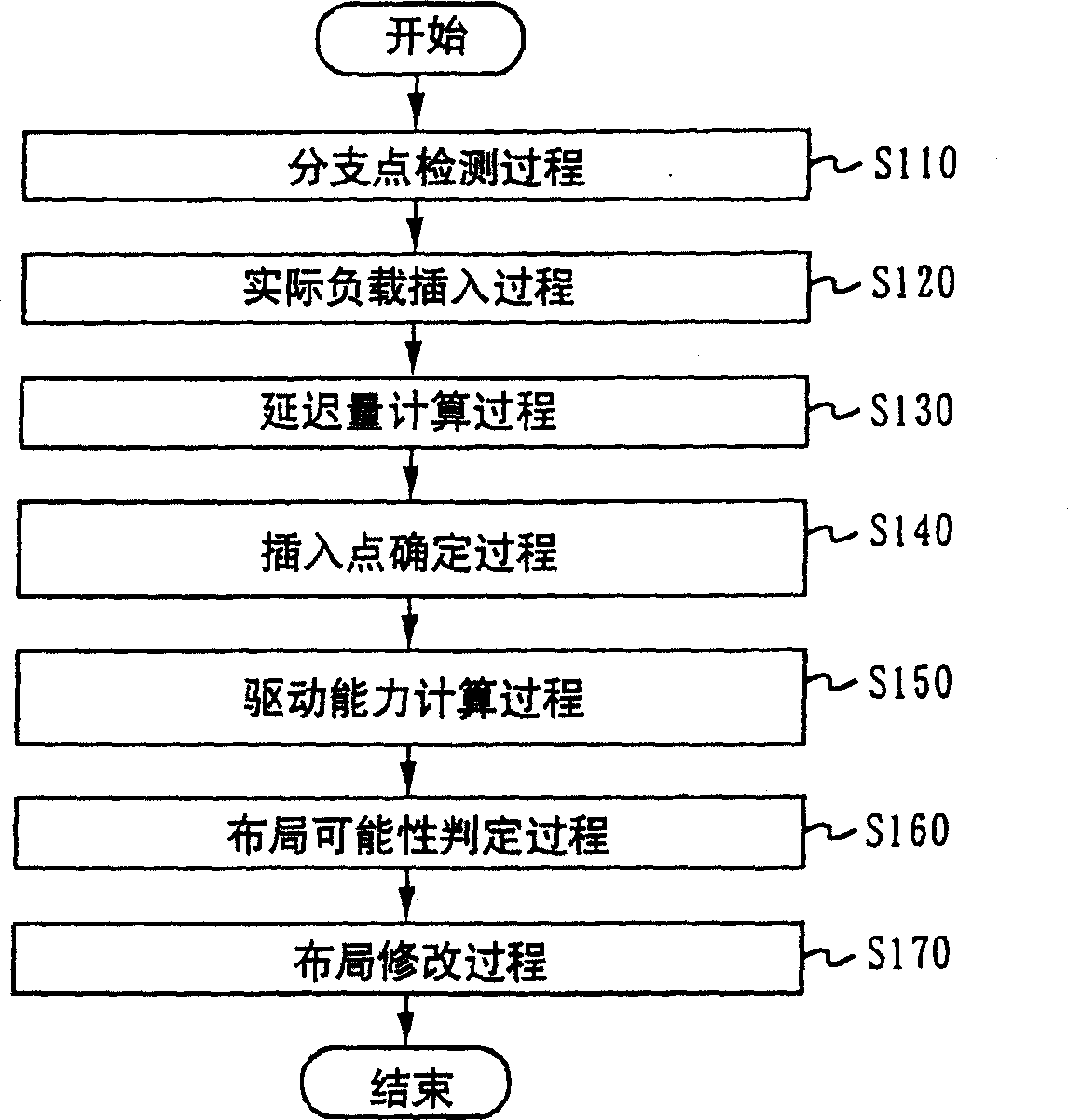
[0049] refer to figure 1 Through 8, the design method according to the first embodiment of the present invention is described. figure 1 is a process flowchart of the design method according to the first embodiment of the present invention. The design method includes a branch point detection process S110, an actual load insertion process S120, a delay amount calculation process S130, an insertion point determination process S140, a driving capability calculation process S150, a layout possibility determination process S160, and a layout modification process S170.

[0050] In the branch point detection process S110, the design tool detects branch points of wiring in the layout results to be processed. Next, in the actual load insertion process S120, for each branch point detected in the branch point detection process S110, the design tool actually inserts a load having a predetermined amount (the load is hereinafter referred to as a virtual buffer) one at a time in the actual...

no. 2 example

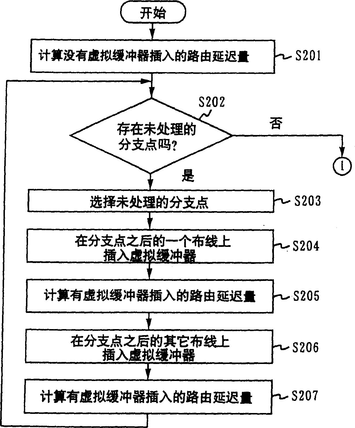
[0098] refer to Figure 9 and 10 , the second embodiment of the present invention will be described below. Figure 9 is a process flowchart of the design method according to the second embodiment of the present invention. By replacing the design method ( figure 1 ) in the actual load insertion process S120 to obtain the design method. exist Figure 9 in the process shown, with figure 1 The same processes as those shown in are given the same reference numerals and are not described again here.

[0099] In the actual load insertion process S121, the design tool determines whether a dummy buffer is required according to a predetermined standard, and then inserts the dummy buffer into the wiring after the branch point detected in the branch point detection process S110 according to the determination that the dummy buffer is required. at the predetermined point above. The actual load insertion process S121 according to the present embodiment includes a total post-branching...

no. 3 example

[0106] refer to Figure 10 and 11 , the third embodiment of the present invention will be described below. Figure 11 is a process flowchart of the design method according to the third embodiment of the present invention. By replacing the design method ( figure 1 ) in the actual load insertion process S120 to obtain the design method. exist Figure 11 in the process shown, with figure 1 The same processes as those shown in are given the same reference numerals and are not described again here.

[0107] Like the actual load insertion process S121 according to the second embodiment, in the actual load insertion process S122, the design tool determines whether a dummy buffer is required according to a predetermined standard, and then inserts the dummy buffer in the At a predetermined point on the wiring after the branch point detected in the branch point detection process S110. The actual load insertion process S122 according to the present embodiment includes a branch-b...


PUM


Abstract

A branching point on a wire is detected in the layout results S101. A delay amount of a route with a dummy buffer being inserted on a wire subsequent to the branching point S102 and that of the route without a dummy buffer being inserted are then calculated S103. Based on the delay amounts, an insertion point at which a load-dividing buffer is to be inserted is determined S104. On condition that a load-dividing buffer is to be inserted at the insertion point, the drive capability of a driving cell preceding the insertion point is calculated so that timing constraints are satisfied S105. Then, after it is confirmed that a load-dividing buffer is insertable at the determined insertion point S106, processes of placing a load-dividing buffer, changing the drive capability of the driving cell, and changing wiring information are performed on the layout results S107.

Description

technical field [0001] The present invention relates to a method of designing a low power consumption semiconductor integrated circuit. More particularly, the present invention relates to a method of designing a low power consumption semiconductor integrated circuit by changing a circuit layout result obtained using a top-down design method. technical background [0002] In recent years, most logic LSIs (Very Large Scale Integration) are designed by using a top-down design method. Top-down design methods generally include functional design process, logic synthesis process and automatic layout process. During the functional design process, the designer uses a hardware description language (HDL) to functionally describe the circuit to be designed. During logic synthesis, a functionally described circuit is converted into gate-level circuit data. In the automatic layout process, a designer uses an automatic layout tool based on gate-level circuit data to obtain layout result...

Claims


Application Information

Patent Timeline
Patent Type & Authority Applications(China)
IPC IPC(8): G06F17/50G06F9/455H01L21/44H01L21/82
CPCG06F17/505G06F17/5068G06F30/39G06F30/327
Inventor 藤田光俊近藤秀二
Owner PANASONIC CORP
Why Eureka
Try Eureka