Display device and driving method thereof

A technology of a display device and a driving method, applied in static indicators, nonlinear optics, instruments, etc., capable of solving problems such as uneven display of display panels, low display panel display, and low brightness of pixel units, so as to avoid uneven display , Reduce the effect of brightness difference

Pending Publication Date: 2021-09-28
SHENZHEN CHINA STAR OPTOELECTRONICS TECH CO LTD
View PDF6 Cites 2 Cited by
  • Summary
  • Abstract
  • Description
  • Claims
  • Application Information

AI Technical Summary

Problems solved by technology

[0002] At present, with the improvement of the resolution, size and refresh rate of the display panel, not only will the charging time of each pixel unit in the display panel become shorter and shorter, but also because the pixel unit close to the source driver is far away from the source driver The capacitive resistance load (RC loding) of the input channel corresponding to the pixel unit is getting larger and larger, so that the charging time from the pixel unit close to the source driver to the pixel unit far away from the source driver is getting shorter and shorter. The brightness of the pixel cell to the pixel cell farther away from the source driver is getting lower and lower, such as figure 1 It is a schematic structural diagram of a display device in the prior art, and if the display panel exists figure 1 The four horizontal display areas shown are: area 1, area 2, area 3 and area 4, the brightness of area 1 to area 4 will be lower and lower, resulting in uneven display of the display panel
[0003] Therefore, since the brightness of the horizontal display area close to the source driver to the horizontal display area away from the source driver is getting lower and lower, the display panel has uneven display, which is the current large-size, high-resolution and high-refresh-rate technology. Display panels increasingly need to solve technical problems

Method used


Image

  • Display device and driving method thereof
  • Display device and driving method thereof
  • Display device and driving method thereof

Examples


Embodiment Construction

[0026] The technical solutions in the embodiments of the present application will be clearly and completely described below in conjunction with the drawings in the embodiments of the present application. Apparently, the described embodiments are only some of the embodiments of this application, not all of them. Based on the embodiments in this application, all other embodiments obtained by those skilled in the art without making creative efforts belong to the scope of protection of this application.

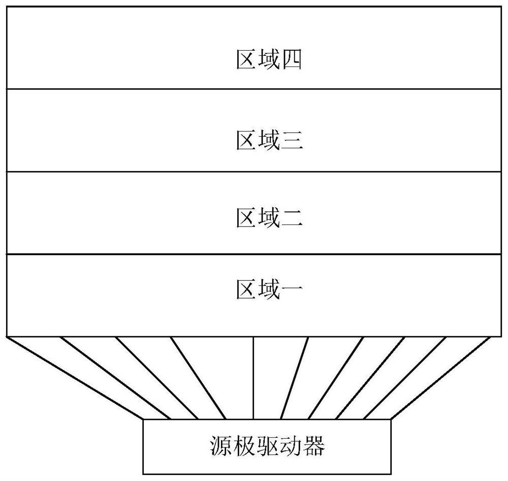
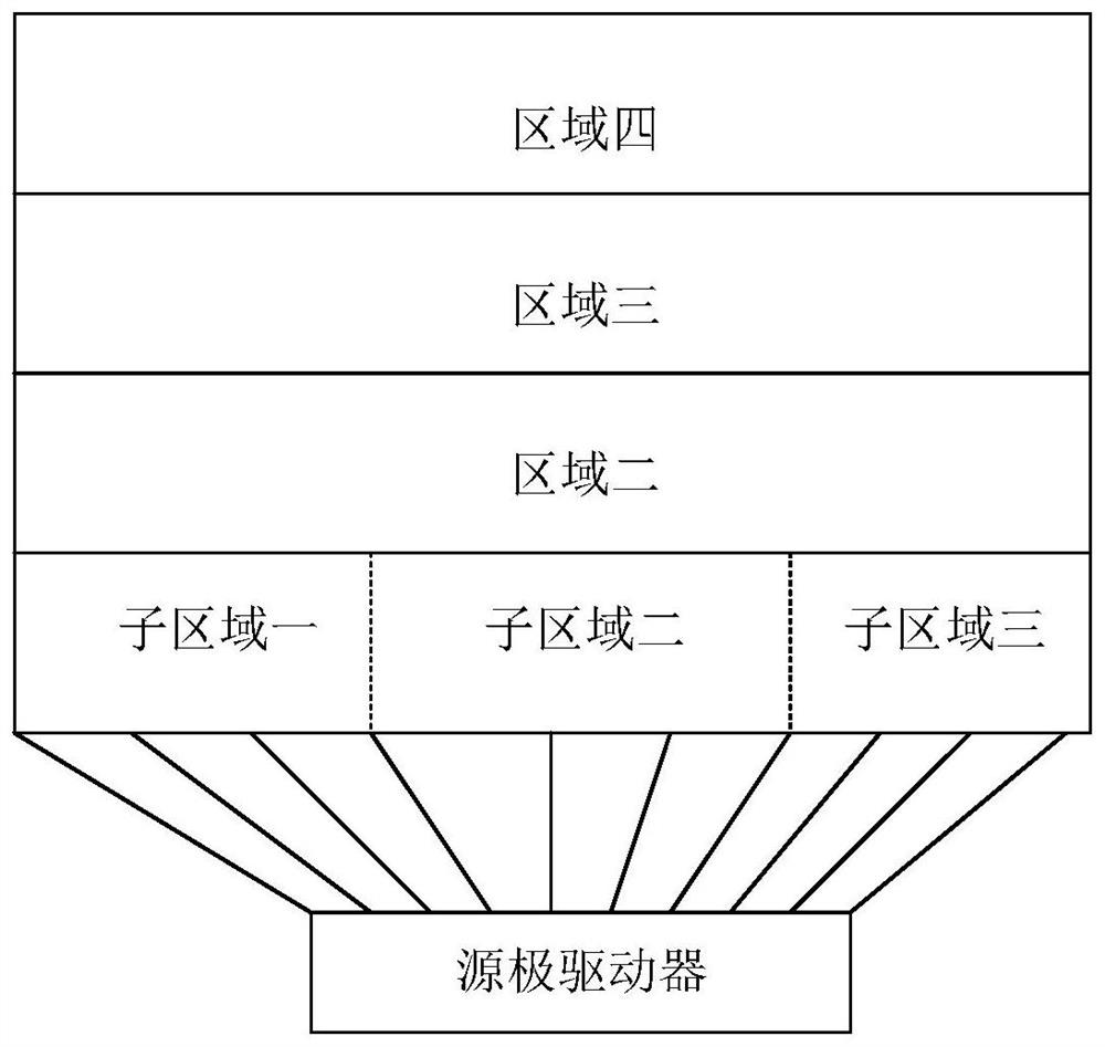
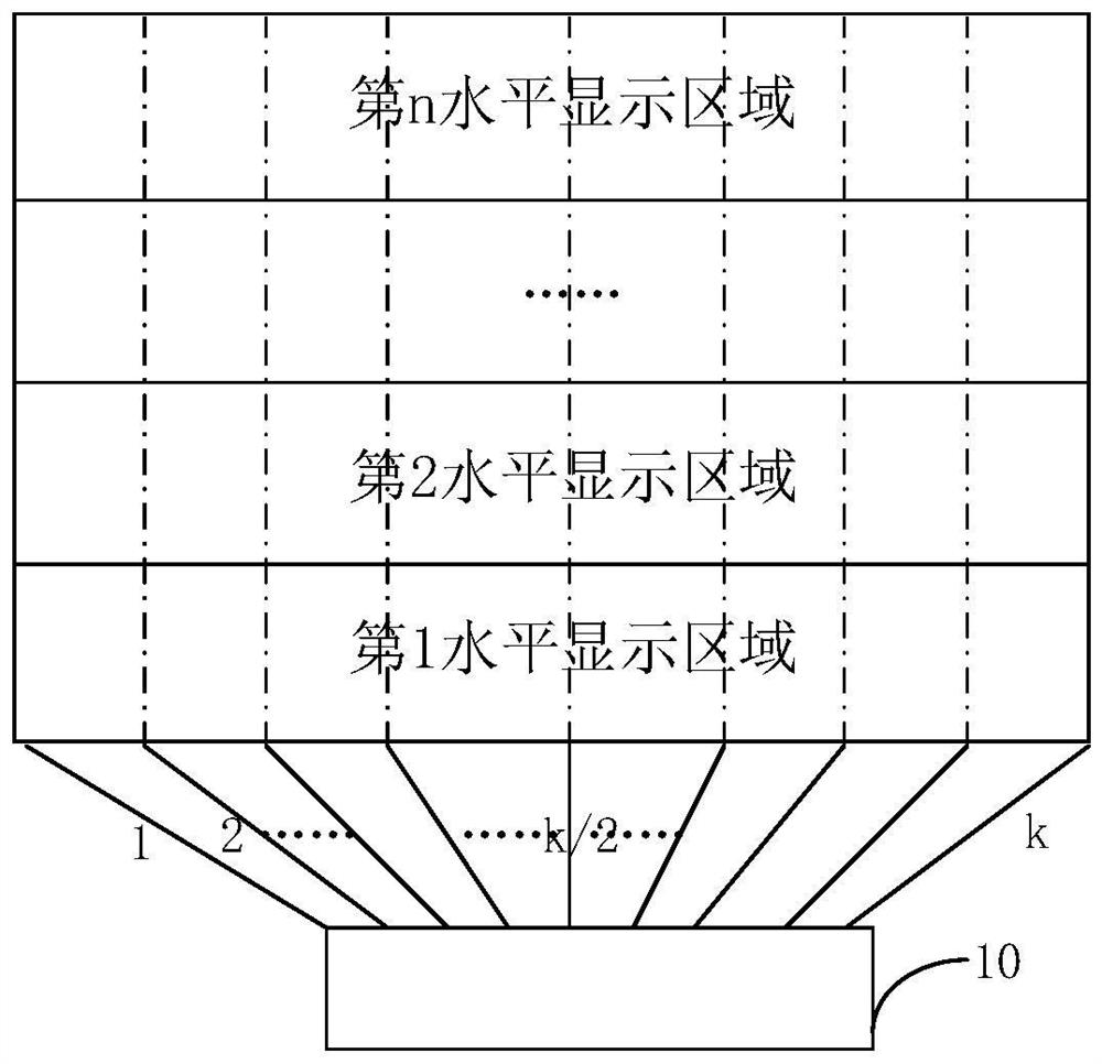
[0027] First of all, since the capacitive resistance load (RC loding) of the input channel corresponding to the pixel unit close to the source driver to the pixel unit far away from the source driver is getting larger and larger, the pixel unit close to the source driver to the pixel far away from the source driver The charging time of the unit is getting shorter and shorter, so the brightness of the pixel unit near the source driver to the pixel unit farther away from the source...


PUM


Abstract

The invention provides a display device and a driving method thereof, and the method comprises the steps: inputting a small-to-large driving current interval into a plurality of horizontal display regions from a position close to a source electrode driver to a position far away from the source electrode driver, so as to achieve the small-to-large driving capability of the plurality of horizontal display regions; therefore, the problem that the brightness is gradually reduced due to the gradually-increased capacitance-resistance load of the horizontal display areas from the position close to the source electrode driver to the position far away from the source electrode driver is solved, the brightness difference between the horizontal display areas is reduced, the brightness of the horizontal display areas is basically the same, and the phenomenon of non-uniform display of the display panel is avoided.

Description

technical field [0001] The present application relates to the field of display technology, in particular to a display device and a driving method thereof. Background technique [0002] At present, with the improvement of the resolution, size and refresh rate of the display panel, not only will the charging time of each pixel unit in the display panel become shorter and shorter, but also because the pixel unit close to the source driver is far away from the source driver The capacitive resistance load (RC loding) of the input channel corresponding to the pixel unit is getting larger and larger, so that the charging time from the pixel unit close to the source driver to the pixel unit far away from the source driver is getting shorter and shorter. The brightness of the pixel cell to the pixel cell farther away from the source driver is getting lower and lower, such as figure 1 It is a schematic structural diagram of a display device in the prior art, and if the display panel ...

Claims


Application Information

Patent Timeline
Patent Type & Authority Applications(China)
IPC IPC(8): G09G3/36G02F1/1345
CPCG09G3/3688G02F1/13452G09G2320/0233G09G2320/0223
Inventor 李文芳
Owner SHENZHEN CHINA STAR OPTOELECTRONICS TECH CO LTD
Why Eureka
Try Eureka