Wafer processing method
A processing method and wafer technology, which can be used in the manufacture of electrical components, electrical solid devices, semiconductor/solid devices, etc., and can solve the problems of device chip quality degradation and other issues
- Summary
- Abstract
- Description
- Claims
- Application Information
AI Technical Summary
Problems solved by technology
Method used
Image

Examples
Embodiment Construction
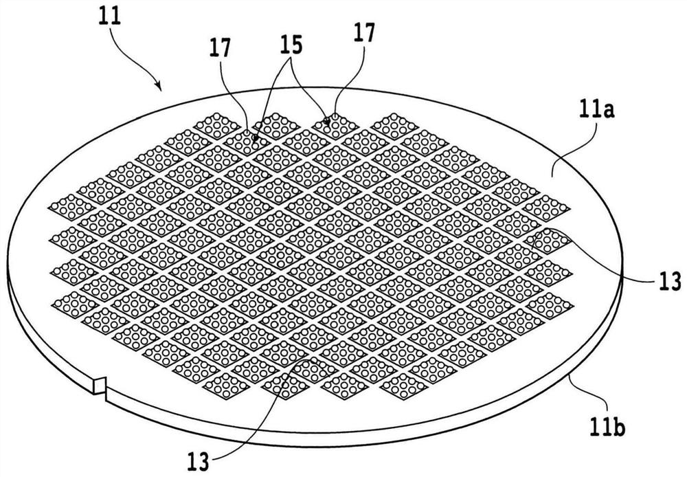
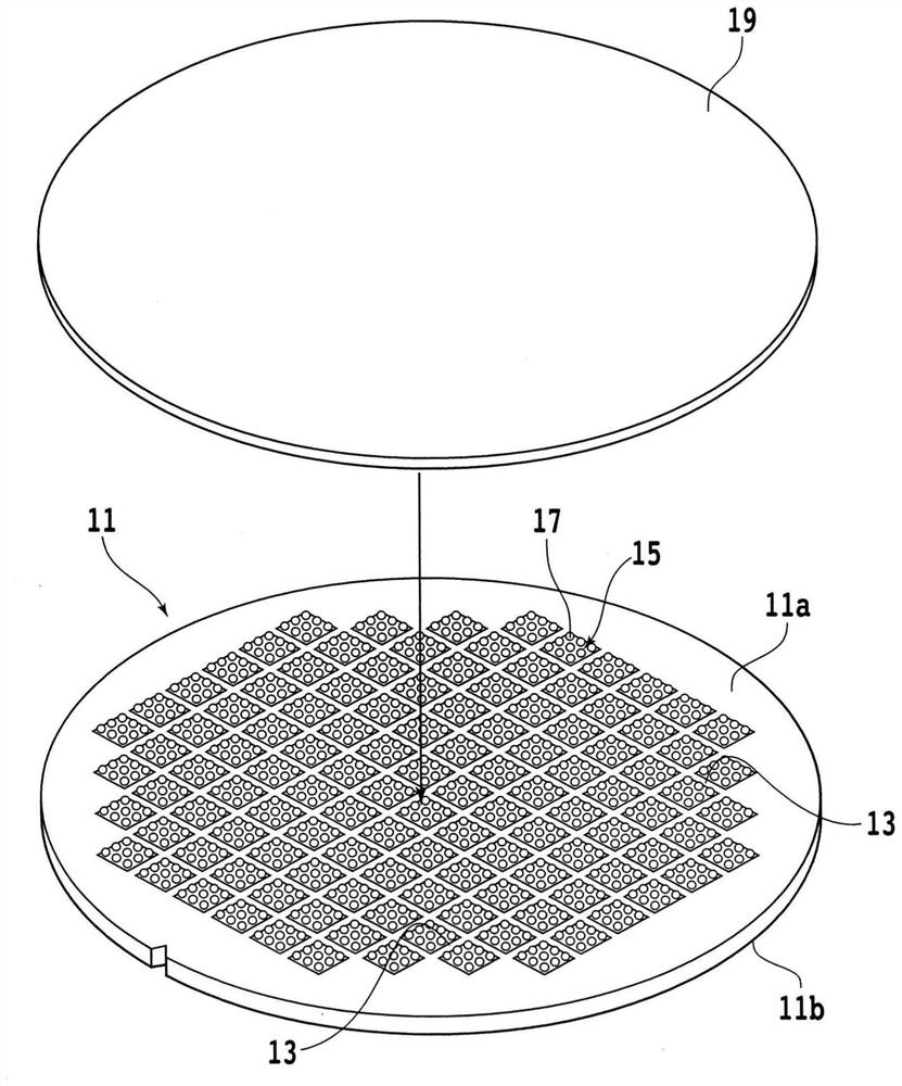
[0029] Hereinafter, an embodiment of one aspect of the present invention will be described with reference to the drawings. First, a configuration example of a wafer processed by the wafer processing method of this embodiment will be described. figure 1 is a perspective view showing the wafer 11 .
[0030] The wafer 11 is, for example, a disk-shaped substrate formed of a semiconductor such as silicon, and has a front surface (first surface) 11a and a rear surface (second surface) 11b substantially parallel to each other. The wafer 11 is divided into a plurality of rectangular regions by a plurality of dividing lines (streets) 13 arranged in a grid pattern so as to intersect each other. In addition, IC (Integrated Circuit, integrated circuit), LSI (Large Scale Integration, large-scale integration), LED (Light Emitting Diode, light emitting diode), MEMS (Micro Electro Mechanical Systems, Micro Electro Mechanical Systems) and other devices 15 .
[0031] In addition, the materia...
PUM
 Abstract
Description
Claims
Application Information
 - R&D
- Intellectual Property
- Life Sciences
- Materials
- Tech Scout
- Unparalleled Data Quality
- Higher Quality Content
- 60% Fewer Hallucinations
Browse by: Latest US Patents, China's latest patents, Technical Efficacy Thesaurus, Application Domain, Technology Topic, Popular Technical Reports.
© 2025 PatSnap. All rights reserved.Legal|Privacy policy|Modern Slavery Act Transparency Statement|Sitemap|About US| Contact US: help@patsnap.com