Package structure where large-size chips are adapted to small-size packages

A technology of small-size packaging and packaging structure, which is applied in the manufacture of semiconductor devices, electric solid-state devices, semiconductor/solid-state devices, etc., can solve the problems of reducing work efficiency, production costs, packaging process difficulty, and process complexity, etc., to save internal space Effect

Active Publication Date: 2022-05-24
SHENZHEN SIPTORY TECH CO LTD
View PDF0 Cites 0 Cited by
  • Summary
  • Abstract
  • Description
  • Claims
  • Application Information

AI Technical Summary

Problems solved by technology

There is a certain conflict between the two: how to package a chip with a larger area in a small package size to meet higher performance requirements
like figure 2 As shown, there are also packaging structures for chips with larger areas through complex multi-layer routing. At least 2 layers of routing need to be connected with complex vias. It is more difficult, the process is complicated, the work efficiency is reduced and the production cost of the product is increased.

Method used


Image

  • Package structure where large-size chips are adapted to small-size packages
  • Package structure where large-size chips are adapted to small-size packages
  • Package structure where large-size chips are adapted to small-size packages

Examples


Embodiment Construction

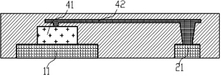
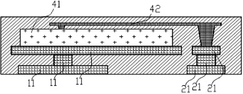
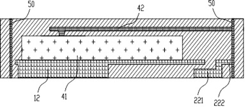
[0049] The technical solutions in the embodiments of the present application will be clearly and completely described below with reference to the accompanying drawings in the embodiments of the present application. Obviously, the described embodiments are only a part of the embodiments of the present application, but not all of the embodiments. Based on the embodiments in this application, all other embodiments obtained by those skilled in the art without creative efforts shall fall within the protection scope of this application.

[0050]In the description of the present application, it should be understood that the terms "first" and "second" are only used for description purposes, and cannot be interpreted as indicating or implying relative importance or implicitly indicating the number of indicated technical features. Thus, features defined as "first", "second" may expressly or implicitly include one or more of said features. In the description of the present application, ...


PUM


Abstract

The present application discloses a package structure in which a large-size chip fits into a small-size package, including a frame, a first pad cavity and a second pad cavity provided in the frame, and a pad cavity provided in the first pad. The chip cavity above the disc cavity, the channel opened on the near side of the frame, the first pad cavity and the second pad cavity are crossed and misaligned, and the channel is located between the two pad cavities On one side, the inner wall surface of the channel is a metallized hole wall; wherein, the first pad cavity, the second pad cavity and the chip cavity are respectively used to accommodate the first pad, the second pads and chips. The large-size chip provided by this application is adapted to the package structure of a small-size package. By setting a channel with a metallized hole wall on the near side of the package structure, more accommodation space is provided for the chip, which effectively improves the packaging structure. Chips account for 60%‑70%, which meets the processing needs of large-size chips to fit small-size packages.

Description

technical field [0001] The present application relates to the technical field of chip packaging, and in particular, to a packaging structure in which a large-sized chip is adapted to a small-sized package body. Background technique [0002] With the development of the semiconductor industry, on the one hand, the performance, power and other parameters of the chip have been greatly improved with the increase of the chip area size, on the other hand, with the development of equipment miniaturization, the package size of the product has become smaller and smaller. There is a certain conflict between the two: how to package a larger area chip in a small package size to meet higher performance requirements. [0003] The current common product packaging structure, such as figure 1 As shown in the figure, the package body is provided with a first pad initial cavity 11, a second pad initial cavity 21, a chip cavity 41, and the first pad, the second pad and the chip corresponding to...

Claims


Application Information

Patent Timeline
Patent Type & Authority Patents(China)
IPC IPC(8): H01L23/48H01L23/49H01L23/488H01L23/31H01L21/56
CPCH01L23/481H01L23/49H01L23/488H01L23/3114H01L21/56H01L2224/24
Inventor 邵冬冬
Owner SHENZHEN SIPTORY TECH CO LTD
Why Eureka
Try Eureka