Substrate bonding apparatus and substrate bonding method

A bonding device and bonding method technology, which is applied in the manufacture of electrical components, circuits, semiconductors/solid-state devices, etc., can solve the problems of reducing the efficiency of bonding devices, vertical alignment deviation, alignment misalignment or distortion, etc., and achieve the effect of reducing coordinate errors

Pending Publication Date: 2022-07-01
TES CO LTD
View PDF0 Cites 0 Cited by
  • Summary
  • Abstract
  • Description
  • Claims
  • Application Information

AI Technical Summary

Problems solved by technology

However, in the case of the conventional device, the upper camera and the lower camera move repeatedly in the horizontal direction or the vertical direction, and the vertical arrangement of the upper camera and the lower camera is misaligned or distorted, and coordinate errors frequently occur.
[0007] And, in the prior art device, the vertical arrangement of the upper camera and the lower camera depends on the operator's manual work, and the deviation of the vertical arrangement greatly occurs according to the operator's proficiency, and the vertical arrangement is carried out by manual work. directional alignment, which greatly reduces the efficiency of the bonding device

Method used


Image

  • Substrate bonding apparatus and substrate bonding method
  • Substrate bonding apparatus and substrate bonding method
  • Substrate bonding apparatus and substrate bonding method

Examples


Embodiment Construction

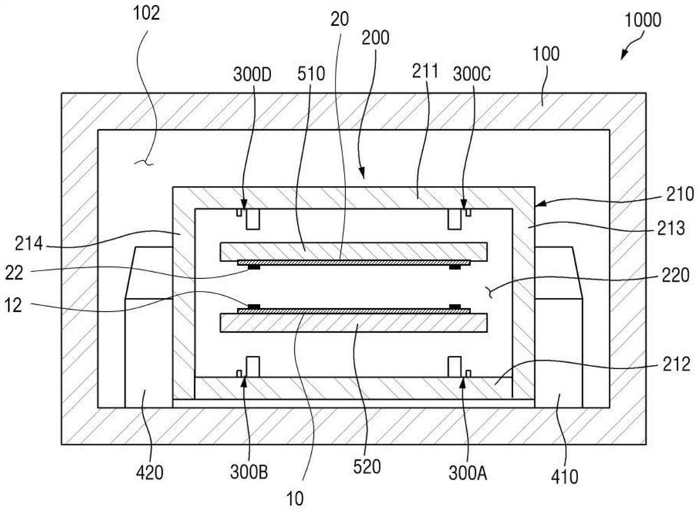
[0047] Hereinafter, the structure of the substrate bonding apparatus and the substrate bonding method according to the embodiment of the present invention will be specifically described with reference to the accompanying drawings.

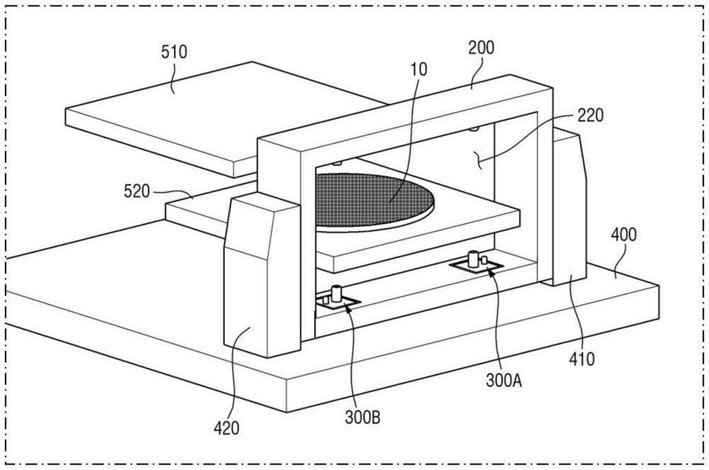
[0048] figure 1 It is a side view of a substrate bonding apparatus 1000 according to an embodiment of the present invention, figure 2 for display figure 1 A perspective view of the internal structure of the substrate bonding apparatus 1000 shown.

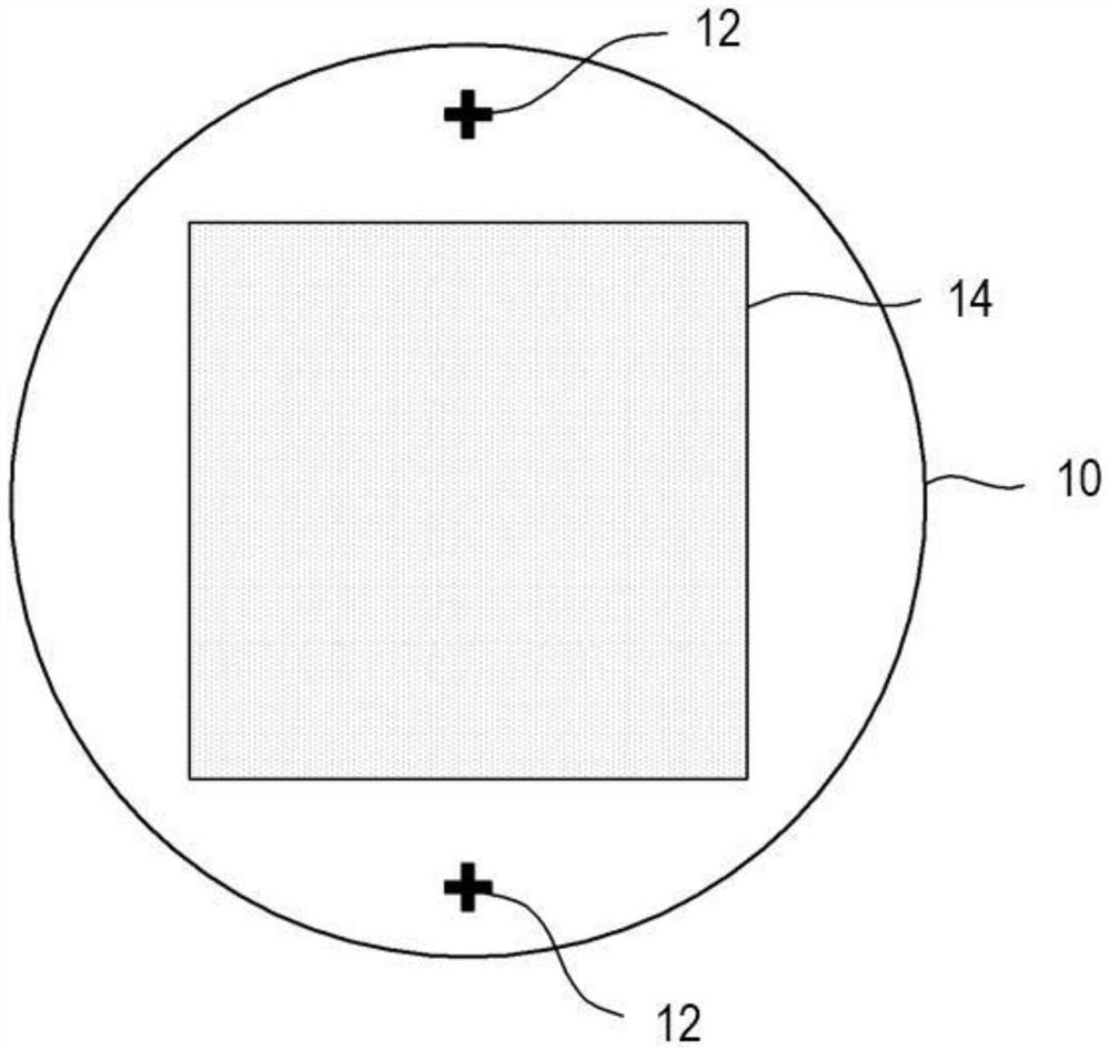
[0049] refer to figure 1 and figure 2 , the substrate bonding apparatus 1000 includes: a cavity 100 ; a first chuck 520 , which is arranged inside the cavity 100 to adsorb the first substrate 10 ; a second chuck 510 to face the first chuck 520 is arranged inside the cavity 100 in a manner of moving vertically and horizontally relative to the first chuck 520 to adsorb the second substrate 20; and the arrangement module 200 has the function of identifying the first chuck 520. The first sorting key 1...


PUM


Abstract

The present invention provides a substrate bonding apparatus and a substrate bonding method, and more particularly, to a substrate bonding apparatus and a substrate bonding method that reduce poor bonding of substrates when the substrates are bonded to each other.

Description

technical field [0001] The present invention relates to a board bonding apparatus and a board bonding method, and more particularly, to a board bonding apparatus and a board bonding method that reduce bonding defects of the boards when the boards are bonded to each other. Background technique [0002] Recently, with the development of technology and industry, there has been an increasing demand for high integration of semiconductor devices or substrates (hereinafter referred to as "substrates"). In this case, when a highly integrated substrate is arranged in a horizontal plane and is commercialized by wiring connection, problems such as increase in wiring length, increase in wiring impedance, and wiring delay arise. [0003] Therefore, a three-dimensional integration technique using three-dimensional stacking of substrates has been proposed. In this three-dimensional integration technique, for example, bonding of the upper and lower substrates is performed using a bonding a...

Claims


Application Information

Patent Timeline
Patent Type & Authority Applications(China)
IPC IPC(8): H01L21/683H01L21/67
CPCH01L21/6838H01L21/67276H01L21/67259
Inventor 金宰焕
Owner TES CO LTD
Why Eureka
Try Eureka