Structure of nonvolatile memory cell

A non-volatile memory and memory cell technology, applied in the field of structure of non-volatile memory elements, can solve the problems of reducing component speed, limiting performance, increasing the area of ​​diffusion area, etc., to increase margin and overcome alignment errors , The effect of reducing chip resistance

Inactive Publication Date: 2006-09-13
MACRONIX INT CO LTD
View PDF0 Cites 0 Cited by
  • Summary
  • Abstract
  • Description
  • Claims
  • Application Information

AI Technical Summary

Problems solved by technology

In the development process of integrated circuits, when the component size advances to the sub-micron technical level, the traditional contact window is not only gradually insufficient, but also limits the performance of the component in many ways
When the area of ​​the contact window shrinks with the size of the device, its resistance also increases. Especially when the diffusion area shrinks with the size of the device, the alignment of the contact window and the diffusion area becomes a difficult problem. In order to avoid the contact window and the diffusion The misalignment of the area causes process problems and component failure. It is often necessary to reserve space for misalignment that will reduce the integration of components, or to maintain or even increase the area of ​​the diffusion area, but increasing the area of ​​the diffusion area will increase the substrate and diffusion. Junction capacitance between areas, thus reducing component speed

Method used


Image

  • Structure of nonvolatile memory cell
  • Structure of nonvolatile memory cell
  • Structure of nonvolatile memory cell

Examples


Embodiment Construction

[0029] In order to make the above and other objects, features and advantages of the present invention more comprehensible, the preferred embodiments are specifically cited below, together with the accompanying drawings, and are described in detail as follows:

[0030] It should be noted here that the process steps and structures described below do not include the complete process of the integrated circuit. The present invention can be implemented in a variety of integrated circuit process technologies, only those required for an understanding of the present invention are mentioned here. The following will be described in detail according to the accompanying drawings of the present invention. The accompanying drawings are all in simple form, but in fact the structure of the memory assembly is much more complicated.

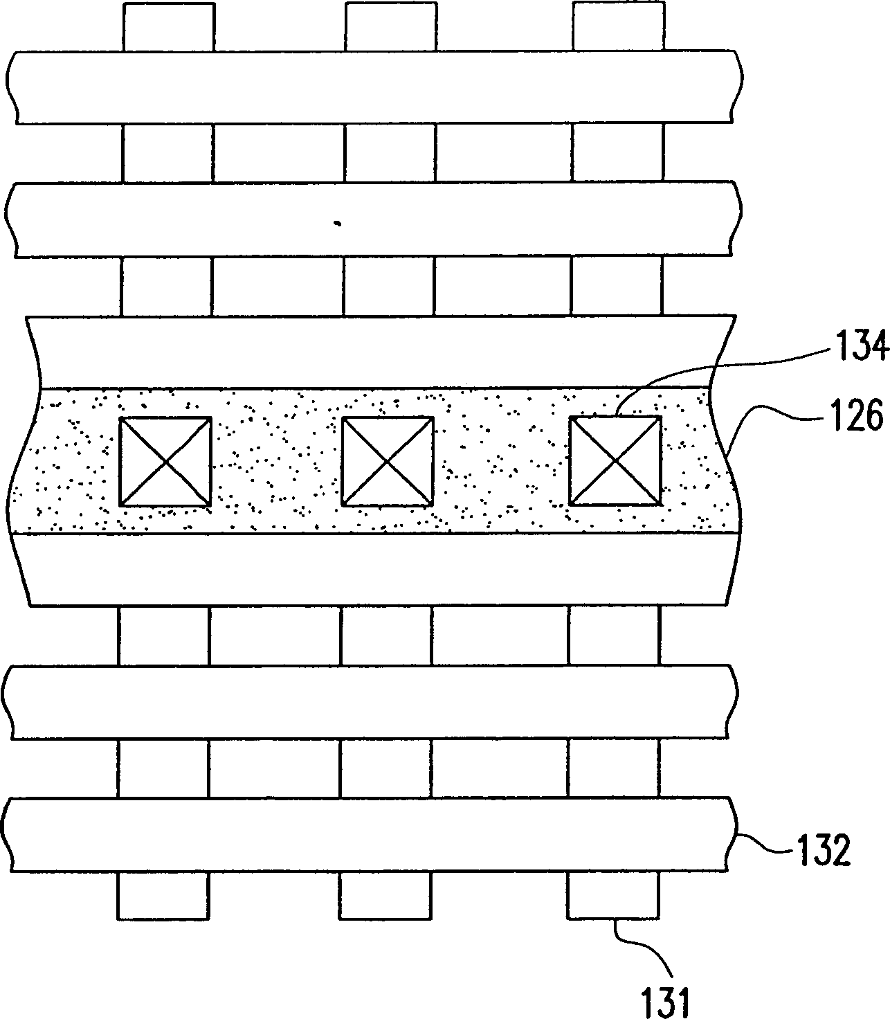
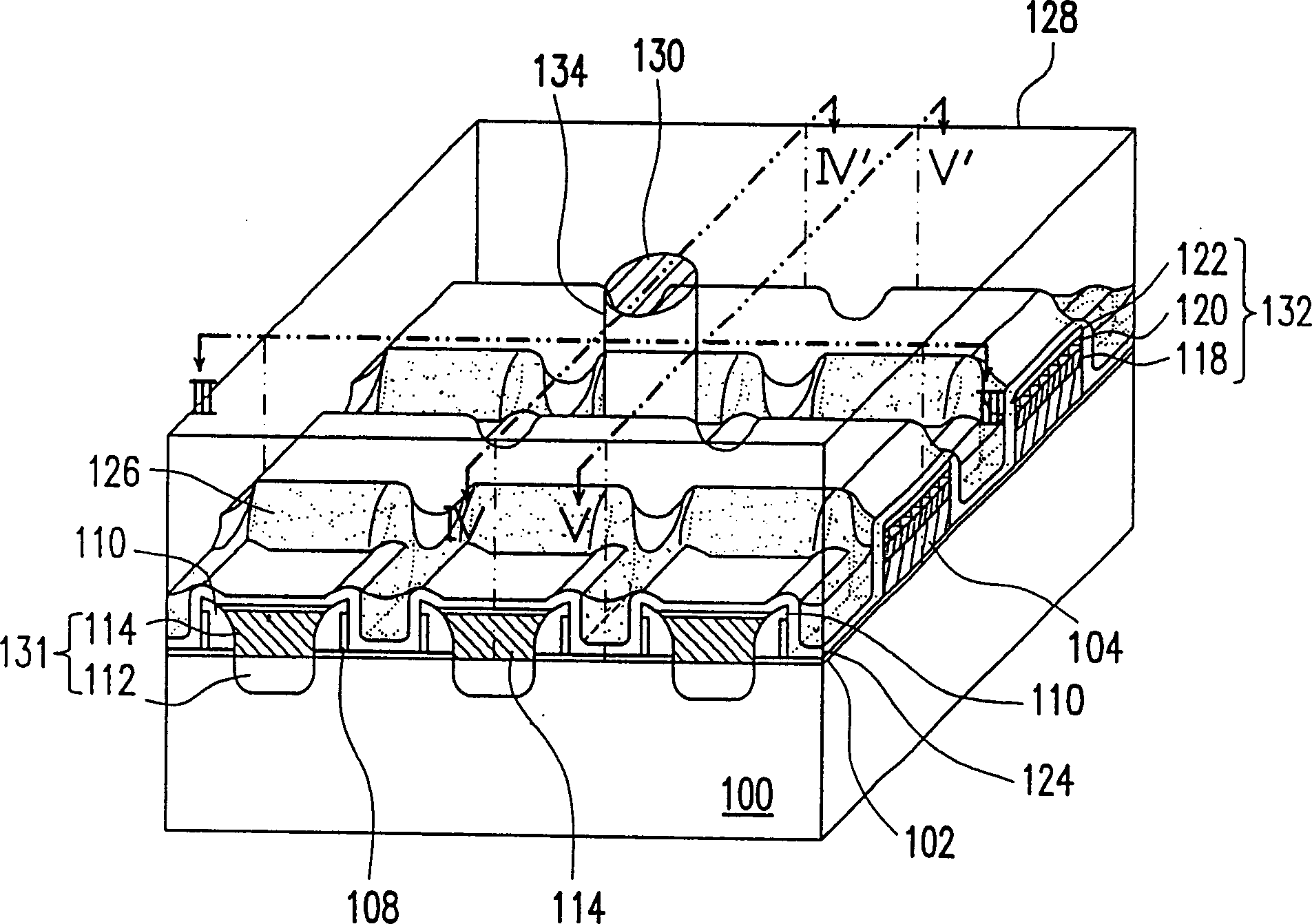
[0031] figure 1 It is a top view of a non-volatile storage element of a preferred embodiment of the present invention, please refer to figure 1 , the structure o...


PUM


Abstract

The memory cell is composed of a grid electrode, a bit line and a word line. The bit line consists of embedded diffused conducting wire and a raised conducting layer on the embedded diffused conducting wire. Grid electrode is located between raised conducting layers of bit line. Word line perpendicular to bit line roughly is located on grid electrode and stepped across raised conducting layers of bit line. Sidewall of raised conducting layers of bit line possesses first gap wall and second gap wall on gap wall of word line.

Description

technical field [0001] The present invention relates to a structure of a memory element, and in particular to a structure of a non-volatile memory element. Background technique [0002] Contacts are used in VLSI and VLSI to connect multilayer circuit structures. In the development process of integrated circuits, when the component size advances to the sub-micron technical level, the traditional contact window is not only gradually insufficient, but also limits the performance of the component in many ways. When the area of ​​the contact window shrinks with the size of the device, its resistance also increases. Especially when the diffusion area shrinks with the size of the device, the alignment of the contact window and the diffusion area becomes a difficult problem. In order to avoid the contact window and the diffusion The misalignment of the area causes process problems and component failure. It is often necessary to reserve space for misalignment that will reduce the in...

Claims


Application Information

Patent Timeline
Patent Type & Authority Patents(China)
IPC IPC(8): H01L27/10
Inventor 林春荣
Owner MACRONIX INT CO LTD
Why Eureka
Try Eureka