MOS devices with improved source/drain regions with SiGe

a technology of source/drain region and mos device, which is applied in the direction of semiconductor devices, electrical devices, transistors, etc., can solve the problems of unfavorable increase in parasitic resistance, and achieve the effect of reducing sheet resistance and reducing silicide region roughness

Inactive Publication Date: 2008-10-30
TAIWAN SEMICON MFG CO LTD
View PDF7 Cites 50 Cited by
  • Summary
  • Abstract
  • Description
  • Claims
  • Application Information

AI Technical Summary

Benefits of technology

[0010]The advantageous features of the present invention include reduced sheet resistance and reduced roughness of silicide regions.

Problems solved by technology

A major problem related to complementary metal oxide silicon (CMOS) scaling is the undesirable increase in parasitic resistance.
Problems occur when the salicide processes are performed on PMOS devices, wherein their source / drain regions are often formed of SiGe.

Method used


Image

  • MOS devices with improved source/drain regions with SiGe
  • MOS devices with improved source/drain regions with SiGe
  • MOS devices with improved source/drain regions with SiGe

Examples


Embodiment Construction

[0013]The making and using of the presently preferred embodiments are discussed in detail below. It should be appreciated, however, that the present invention provides many applicable inventive concepts that can be embodied in a wide variety of specific contexts. The specific embodiments discussed are merely illustrative of specific ways to make and use the invention, and do not limit the scope of the invention.

[0014]A novel method for forming silicon germanium (SiGe) regions in metal-oxide-semiconductor (MOS) devices is provided. The intermediate stages of manufacturing a preferred embodiment of the present invention are illustrated in FIGS. 1 through 9. Variations of the preferred embodiments are then discussed. Throughout the various views and illustrative embodiments of the present invention, like reference numbers are used to designate like elements.

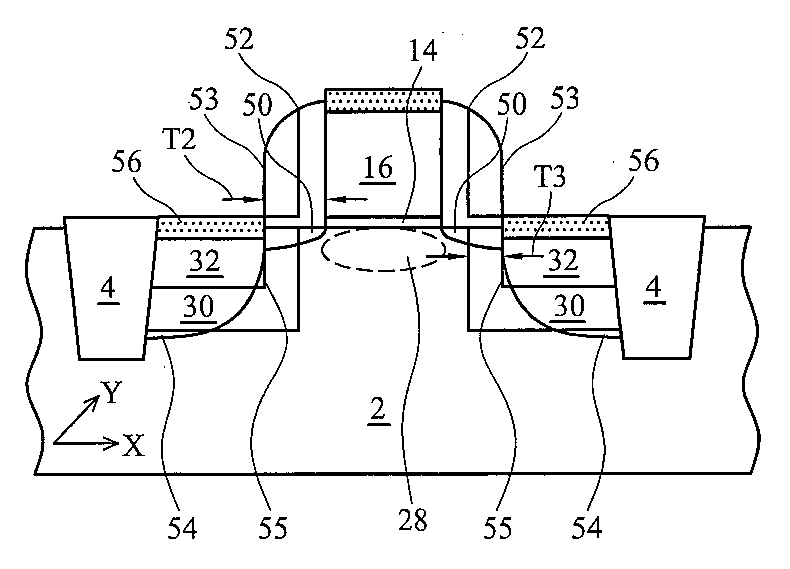
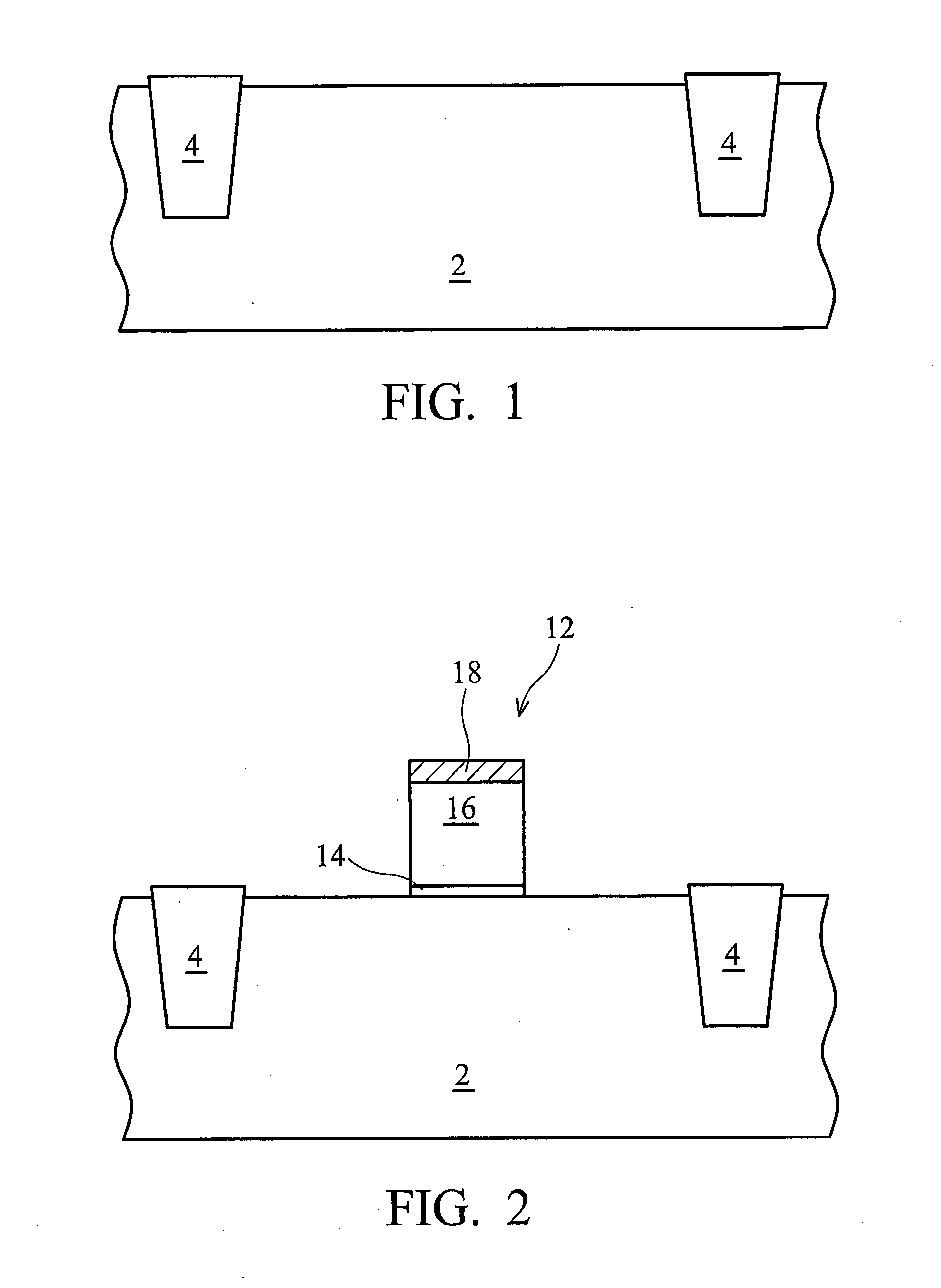
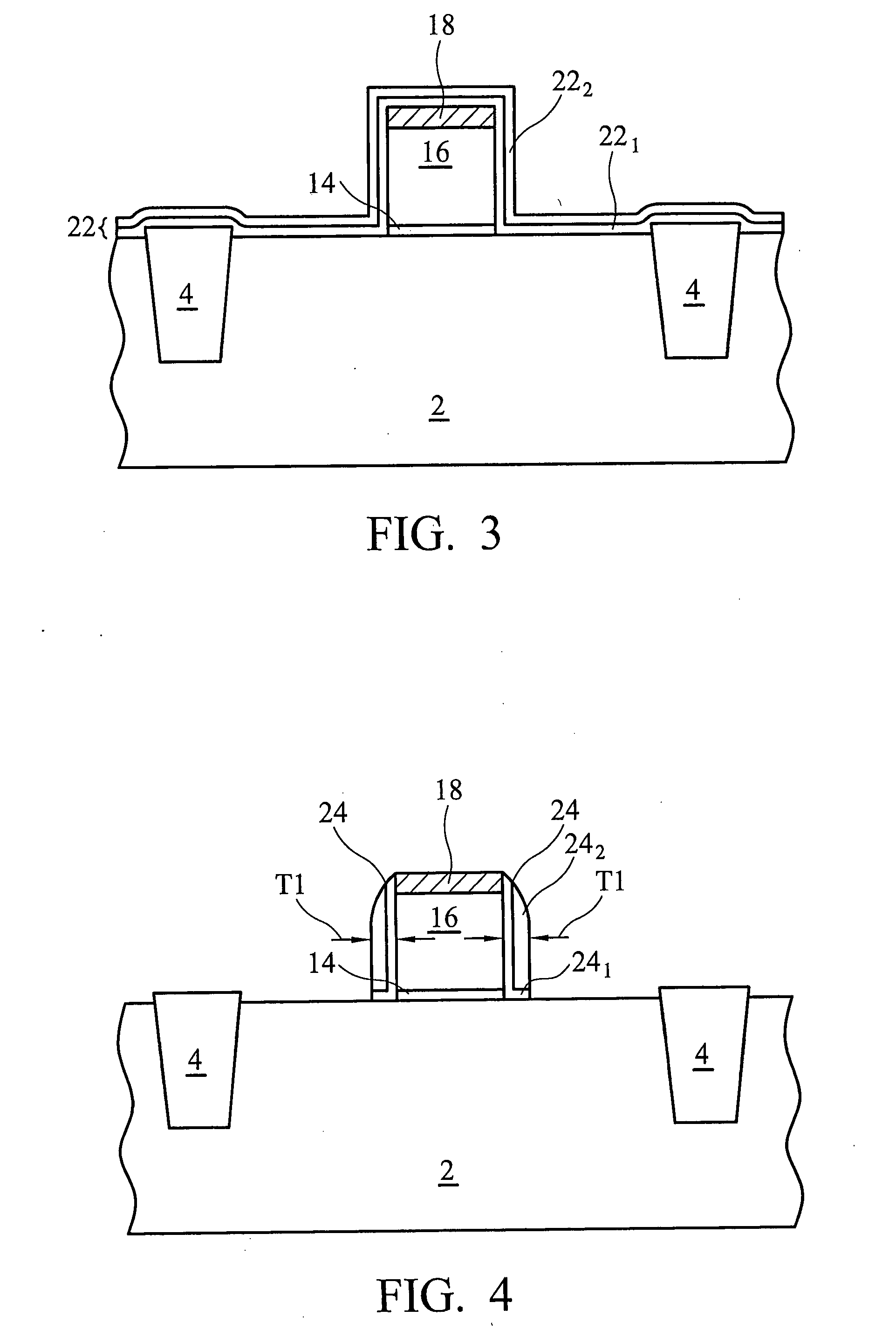
[0015]FIG. 1 illustrates the formation of shallow trench isolation (STI) regions 4 in substrate 2. In the preferred embodiment, su...


PUM


Abstract

A semiconductor structure and methods for forming the same are provided. The semiconductor structure includes a semiconductor substrate; a gate stack on the semiconductor substrate; a SiGe region in the semiconductor substrate and adjacent the gate stack, wherein the SiGe region has a first atomic percentage of germanium to germanium and silicon; and a silicide region over the SiGe region. The silicide region has a second atomic percentage of germanium to germanium and silicon. The second atomic percentage is substantially lower than the first atomic percentage.

Description

TECHNICAL FIELD[0001]This invention relates generally to integrated circuits, and more particularly to structure and formation methods of MOS devices with silicon germanium regions.BACKGROUND[0002]The deep-submicron scaling required for VLSI systems dominates design considerations in the microelectronics industry. As the gate electrode length is scaled down, the source and drain junctions must be scaled down accordingly to suppress the so-called short channel effects (SCE) that degrade performance of miniaturized devices. A major problem related to complementary metal oxide silicon (CMOS) scaling is the undesirable increase in parasitic resistance. As the source / drain junction depth and polycrystalline silicon line width are scaled into the deep-submicron range, contact resistance becomes more significant and needs to be reduced.[0003]The principle way of reducing contact resistances between polysilicon gates and source / drain regions and interconnect lines is by forming metal silici...

Claims


Application Information

Patent Timeline
Patent Type & Authority Applications(United States)
IPC IPC(8): H01L29/94
CPCH01L29/165H01L29/665H01L29/6656H01L29/6659H01L29/66636H01L29/7833H01L29/7848
Inventor LIN, CHUN-CHIEHHSU, WEI-HUACHANG, YU-EN PERCYCHANG, CHUNG LICHENG, CHI-FENGHUNG, WINKO, KISHIMOTO
Owner TAIWAN SEMICON MFG CO LTD
Why Eureka
Try Eureka