Display with function of initializing brightness data of optical elements

A technology of optical components and brightness data, applied in static indicators, cathode ray tube indicators, instruments, etc., can solve problems such as incomplete charge leakage, residual images, and ugly images

Inactive Publication Date: 2003-05-14
SANYO ELECTRIC CO LTD
View PDF0 Cites 50 Cited by
  • Summary
  • Abstract
  • Description
  • Claims
  • Application Information

AI Technical Summary

Problems solved by technology

[0006] When setting large luminance data to optical elements or drive transistors, attempts to set smaller luminance data by rewriting the luminance data will often eventually lead to residual image phenomena, incomplete leakage of charge corresponding to the previous large luminance data remaining in the optical element, Therefore, the required brightness data cannot be set accurately
This makes it hard to see, especially if you're going to show fast-moving footage.

Method used


Image

  • Display with function of initializing brightness data of optical elements
  • Display with function of initializing brightness data of optical elements
  • Display with function of initializing brightness data of optical elements

Examples


no. 1 example

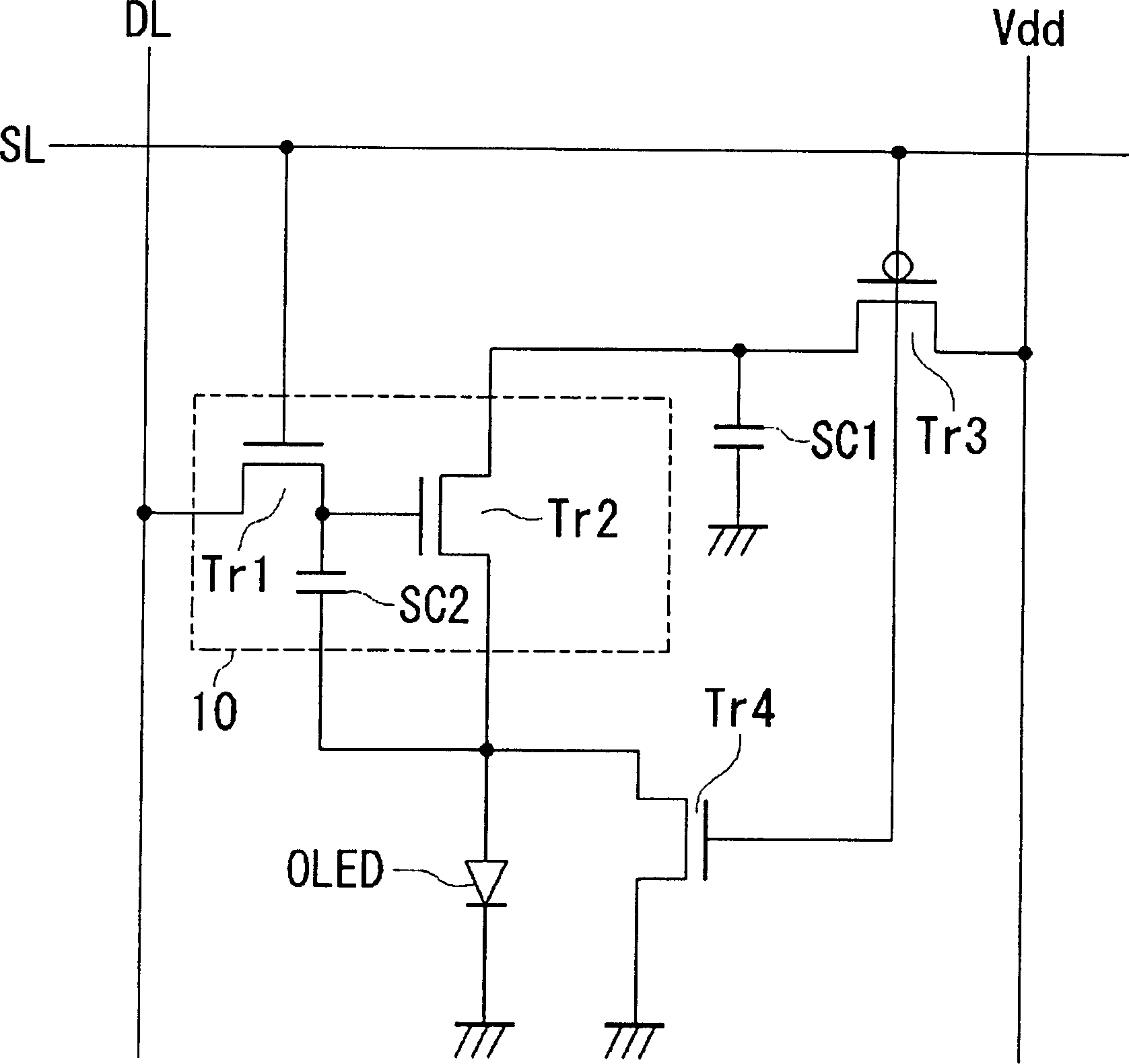
[0062] figure 1 A circuit of a display pixel in the first embodiment of the present invention is shown. The pixel includes an organic light emitting diode OLED (optical element), a driving circuit 10, first and second storage capacitors SC1 and SC2, and fourth and third transistors Tr4 and Tr3 as switching elements. The drive circuit 10 also includes first and second transistors Tr1 and Tr2.

[0063] The pixel also includes a data line DL inputting luminance data, a power line Vdd supplying current to the organic light emitting diode OLED, and a scan line SL inputting a luminance data update signal. The data line DL, the power line Vdd and the scan line SL are shared by other pixels.

[0064] In addition, the first, second and fourth transistors Tr1, Tr2 and Tr4 are n-channel transistors, and the third transistor Tr3 is a p-channel transistor.

[0065] Gates of the first, fourth and third transistors Tr1, Tr4 and Tr3 are all connected to the scan line SL. The drain (or so...

no. 2 example

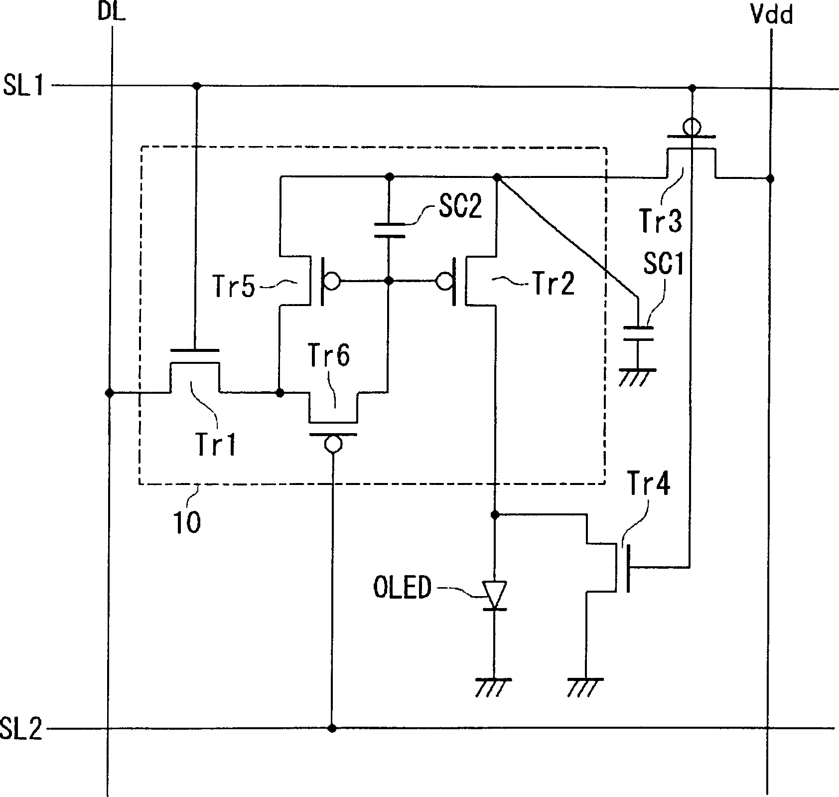
[0071] figure 2 A circuit of a display pixel in the second embodiment of the present invention is shown. The pixel includes an organic light emitting diode OLED (optical element), a drive circuit 10, first and second storage capacitors SC1 and SC2, fourth and third transistors Tr4 and Tr3 as switching elements, a data line DL, a power supply line Vdd, and The first and second scan lines SL1 and SL2. The driving circuit 10 further includes first, second, fifth and sixth transistors Tr1, Tr2, Tr5 and Tr6. The first and fourth transistors Tr1 and Tr4 are n-channel transistors, and the second, third, fifth and sixth transistors Tr1 , Tr3 , Tr5 and Tr6 are p-channel transistors.

[0072] The gates of the first, third and fourth transistors Tr1, Tr3 and Tr4 are all connected to the first scan line SL1, and the gate of the sixth transistor Tr6 is connected to the second scan line SL2. The drain (or source) of the first transistor Tr1 is connected to the data line DL. The source ...

no. 3 example

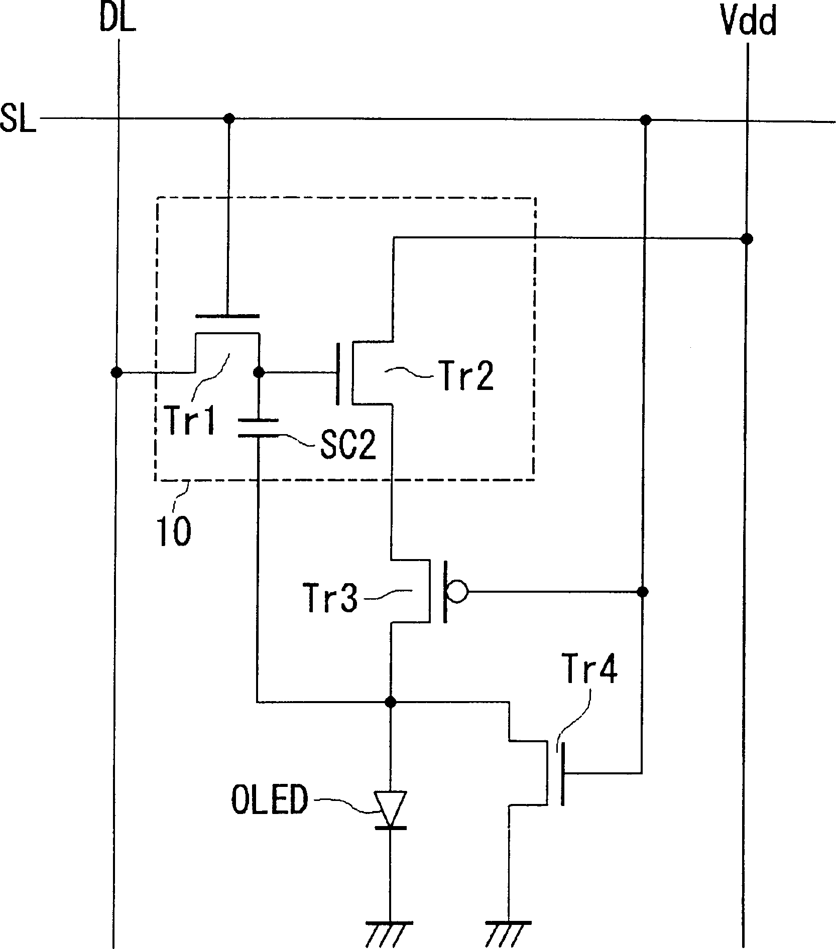
[0077] image 3 with 4 A circuit of a display pixel in a third embodiment of the present invention is shown. In the first and second embodiments, the third transistor Tr3 as a switching element is provided between the power supply line Vdd and the driving circuit 10, but in the third embodiment, the above-mentioned transistor Tr3 is located between the driving circuit 10 and the organic light emitting diode OLED. between. Thus, in image 3 circuit, the first embodiment figure 1 The third and second transistors Tr3 and Tr2 in the circuit are interchanged in connection order. likewise in Figure 4 circuit, the second embodiment figure 2 The connection order of the third and second transistors Tr3 and Tr2 is also interchanged.

[0078] The description of the operating principles of these circuits is omitted here because their operating principles are basically the same as those of the circuits of the first and second embodiments, and the same advantageous effects can be ...


PUM


Abstract

When the scanning line turns high and the first transistor turns on to write luminance data, a potential corresponding to the luminance data in the organic light emitting diode is set in both the gate electrode of the second transistor. At the same time, the fourth transistor turns on, and the electric charge in the anode of the organic light emitting diode is pulled out to ground potential by way of the fourth transistor. Also, at the same time, the third transistor turns off, so that any shoot-through current from the power supply line Vdd will be prevented. Thus the potential at the anode of the organic light emitting diode becomes the same as the ground potential. Thus, the luminance data already present in the optical element is initialized.

Description

technical field [0001] The present invention relates to a display, in particular to a technology for improving display quality of an active matrix display. Background technique [0002] Applications of notebook personal computers and portable terminals are spreading rapidly. The displays mainly used in such devices are liquid crystal displays, but it is organic EL (electroluminescent) displays that are expected to be promising as next-generation display panels. An active matrix driving system is a representative display method of this type of display. A display using this system is called an active matrix display. Many pixels are arranged vertically and horizontally in a matrix, and each pixel is provided with a switching element, which continuously writes image data into each pixel. [0003] After various pixel circuits have been proposed, the research and development of organic EL displays is currently at the beginning stage. An example of this type of circuit is the pi...

Claims


Application Information

Patent Timeline
Patent Type & Authority Applications(China)
IPC IPC(8): G09G3/00G09G3/32
CPCG09G2300/0842G09G2330/021G09G3/3266G09G2300/0876G09G2300/0852G09G2300/0861G09G2320/043G09G2310/0262G09G2300/0809G09G2310/0251G09G3/3241G09G3/3233G09G2310/0256G09G3/2037G09G3/2062G09G5/10G09G2310/0205
Inventor 野口幸宏松本昭一郎土屋博佐野景一
Owner SANYO ELECTRIC CO LTD
Why Eureka
Try Eureka