Input and output combined structure for dielectric-filled waveguide resonator
A technology of input and output, dielectric, applied in the direction of resonators, waveguide devices, circuits, etc., can solve the problems of difficult input and output electrodes, not suitable for mass production, hindering dielectric waveguide resonators, etc.
- Summary
- Abstract
- Description
- Claims
- Application Information
AI Technical Summary
Problems solved by technology
Method used
Image

Examples
Embodiment Construction
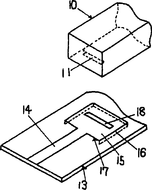
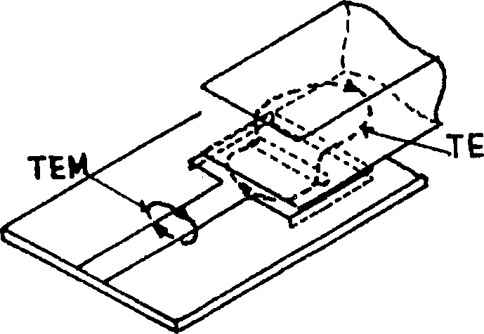
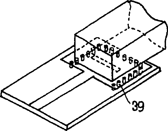
[0026] The TEM mode propagating on the microstrip line is converted to the TE mode by the same mode conversion section provided in the printed circuit board as the microstrip line. Thereafter, a portion of the conductive film on the upper surface of the printed circuit board of the conversion portion is removed to form grooves. Further, a portion of the conductive film on the bottom surface of the dielectric waveguide resonator was removed to form grooves. The grooves formed in this dielectric waveguide resonator are formed to face the grooves of the above-mentioned printed circuit board. By mounting the dielectric waveguide resonator on the groove of the printed substrate, the TE mode in the printed substrate is combined with the TE mode inside the dielectric waveguide resonator. The result is an energy combination between the microwave transmission line and the dielectric waveguide resonator, the two being connected together.
[0027] Embodiments of the present invention w...
PUM
 Abstract
Description
Claims
Application Information
 - R&D Engineer
- R&D Manager
- IP Professional
- Industry Leading Data Capabilities
- Powerful AI technology
- Patent DNA Extraction
Browse by: Latest US Patents, China's latest patents, Technical Efficacy Thesaurus, Application Domain, Technology Topic.
© 2024 PatSnap. All rights reserved.Legal|Privacy policy|Modern Slavery Act Transparency Statement|Sitemap