
Pattern production system, exposure system, and exposure method

A manufacturing system and exposure device technology, which is applied in the direction of photolithography exposure device, radiation-sensitive mask exposure method, printed circuit manufacturing, etc., can solve the problem that the developer or etching solution is slowly degraded, cannot be ignored, and cannot inhibit the finished product Deviation and other issues

Inactive Publication Date: 2005-02-16
FUJIFILM CORP
View PDF5 Cites 6 Cited by
  • Summary
  • Abstract
  • Description
  • Claims
  • Application Information

AI Technical Summary

Problems solved by technology

[0008] However, in the above-mentioned methods of Patent Document 1 and Patent Document 2, the line width of the input data is corrected to make the line width of the finished circuit pattern line close to the specified line width, but due to repeated processing, the developer or etching The liquid gradually deteriorates, and the deviation of the finished product due to its deterioration cannot be suppressed
In addition, in order to suppress the deviation of the finished product caused by the deterioration of the etchant in such a method of manufacturing the photomask, it is necessary to remake the photomask many times, which will increase the production cost.
[0009] And in Patent Document 3, by confirming the change of the amount of etching pattern line, changing the supply of new etchant or spraying pressure, and control etch progress so that finished product is constant, but, in the supply of such new etchant or In the control of the change of the spray pressure, the responsiveness may be unstable, and there may be problems in the deviation of the finished product.
[0010] In addition, in recent years, with the complexity and high precision of circuit patterns, and the pursuit of higher-precision finished products, it is increasingly impossible to ignore such deviations in finished products caused by deterioration of etchant.

Method used


Image

  • Pattern production system, exposure system, and exposure method
  • Pattern production system, exposure system, and exposure method
  • Pattern production system, exposure system, and exposure method

Examples


Embodiment Construction

[0116] Hereinafter, a first embodiment of the pattern creation system of the present invention will be described with reference to the drawings.

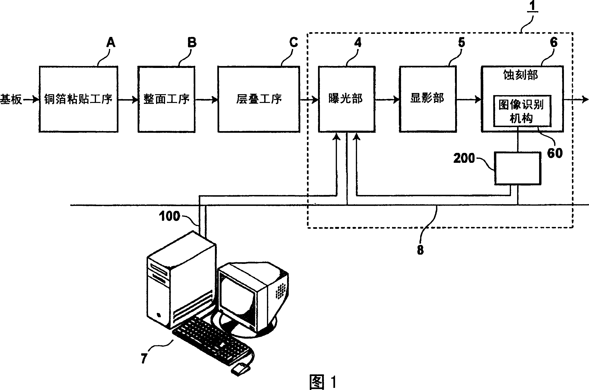
[0117] FIG. 1 is a diagram showing a first embodiment of a pattern manufacturing system, and a case where a circuit pattern as an example of a formed pattern is manufactured by the pattern manufacturing system 1 will be described. When forming a circuit pattern on a substrate, first, in the copper foil pasting process A, copper foil as a circuit forming material is pasted on the substrate, and in the surface preparation process B, the surface of the pasted copper foil is mechanically polished or chemically polished. The upper surface is subjected to surface treatment, and in the lamination step C, a resist (resist material) is laminated on the entire surface of the copper foil upper surface. Secondly, by the pattern manufacturing system 1 of the present invention, the resist coated on the substrate is exposed, and the exposed resist...


PUM


Abstract

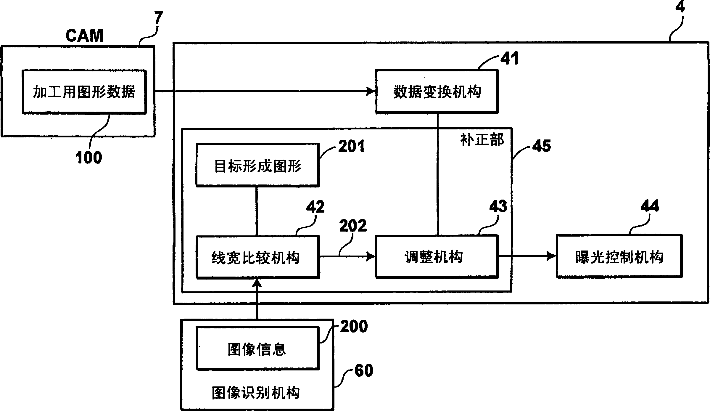
In a pattern production system, resist coated on copper foil on the substrate is exposed to light, by direct drawing, on the basis of a width of a line forming a pattern designated by processing pattern data at a predetermined exposure, the exposed resist is developed to form a resist pattern, and the copper foil is etched to form an etched pattern. An image of the etched pattern is scanned and image information of the etched pattern is obtained. The width of the line forming the pattern represented by the image information and the width of the line forming the pattern of the target etched pattern are compared, and the width of the line forming the pattern designated by the processing pattern data is adjusted on the basis of the result of comparison. The resist is exposed to light, by direct drawing, with the adjusted line width on the basis of the result of comparison.

Description

technical field [0001] The present invention relates to a pattern manufacturing system that suppresses variation in finished products due to deterioration of a developing solution or an etching solution when manufacturing circuit patterns and the like of a printed circuit board. Background technique [0002] For example, in the case of manufacturing a printed substrate, a method has been known in the past: firstly make a photomask, use the photomask to expose and cure the resist on the substrate, and then develop the resist to form a resist. pattern, using the resist pattern to etch the copper foil on the substrate to form a circuit pattern. In the conventional method described above, the amount of copper foil on the substrate varies depending on the density of the resist pattern lines during etching, and there is a problem that the line width of the finished circuit pattern lines varies. Regarding this, there is a method of adjusting pattern lines of a photomask by correct...

Claims


Application Information

Patent Timeline
Patent Type & Authority Applications(China)
IPC IPC(8): G03D5/00G03F1/00G03F7/20G03F7/26H05K1/02H05K3/00H05K3/06
CPCH05K2203/163H05K3/0082H05K1/0269G03F7/2053H05K3/064H05K2203/107G03F7/20
Inventor 森田清辉菅沼敦中谷大辅泽野充
Owner FUJIFILM CORP
Learn More