Unlock instant, AI-driven research and patent intelligence for your innovation.

Method for controlling a recess etch process

A control method and etching technology, applied in semiconductor/solid-state device manufacturing, material analysis through optical means, instruments, etc., can solve the problem that it is difficult to accurately determine the etching depth of columnar polysilicon

Inactive Publication Date: 2005-09-28
LAM RES CORP
View PDF0 Cites 13 Cited by
  • Summary
  • Abstract
  • Description
  • Claims
  • Application Information

AI Technical Summary

Problems solved by technology

Because these variations are unknown, it is difficult to determine precisely how deep the columnar polysilicon should be etched to achieve the desired groove depth

Method used


Image

  • Method for controlling a recess etch process
  • Method for controlling a recess etch process
  • Method for controlling a recess etch process

Examples


Embodiment Construction

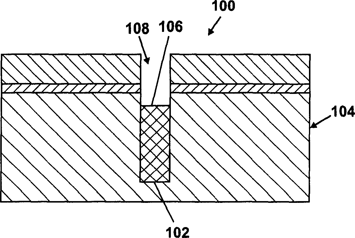
[0037] Now, the invention will be described in detail with reference to some preferred embodiments as shown in the accompanying drawings. In the following description, various details are set forth in order to facilitate a complete understanding of the invention. It will be apparent, however, to one skilled in the art that the present invention may be practiced without all or some of these specific details. In other instances, well known process steps and / or features have not been described in detail in order not to unnecessarily obscure the present invention. The features and advantages of the present invention may be better understood with reference to the drawings and discussion that follow.

[0038] The present invention provides a robust and reliable method for determining the endpoint of the recess etch process. The method of the present invention can be divided into two main steps. In one embodiment, the first step includes estimating changes in the incoming material...


PUM


Abstract

A method of controlling a recess etch process for a multilayered substrate having a trench therein and a column of material deposited in the trench includes determining a first dimension from a surface of the substrate to a reference point in the substrate by obtaining a measured net reflectance of at least a portion of the substrate including the trench, computing a modeled net reflectance of the portion of the substrate as a weighted incoherent sum of reflectances from n1 different regions constituting the portion of the substrate, determining a set of parameters that provides a close match between the measured net reflectance and the modeled net reflectance, and extracting the first dimension from the set of parameters; computing an endpoint of the process as a function of the first dimension and a desired recess depth measured from the reference point; and etching down from a surface of the column of material until the endpoint is reached.

Description

technical field [0001] The present invention generally relates to monitoring and control methods employed during the formation of features on patterned substrates, such as semiconductor substrates. More specifically, the present invention relates to a method for endpoint detection during recess etching. Background technique [0002] Recess etching processes are used in the fabrication of semiconductor devices such as dynamic random access memory (DRAM) and embedded DRAM (eDRAM). DRAM and eDRAM store information in integrated circuits that contain capacitors. Figure 1A A storage junction 100 in a typical DRAM cell is shown. The storage junction 100 includes a deep trench 102 formed in a patterned semiconductor substrate 104 . A columnar polysilicon 106 is formed in the deep trench 102 , and a groove 108 is formed on the columnar polysilicon 106 . Recess 108 may be lined with an insulating material (not shown) to insulate polysilicon 106 from overlying structures (eg, tran...

Claims


Application Information

Patent Timeline
Patent Type & Authority Applications(China)
IPC IPC(8): G01B11/02G01B11/06G01N21/00G01N21/27G01N21/45H01L21/027H01L21/3065H01L21/334H10B12/00
CPCH01L29/66181G01B11/0683H01L27/1087G01B11/0625G01B11/0616H10B12/0387H01L22/00
Inventor 维贾雅库马尔·C·韦努戈帕尔安德鲁·J·佩里
Owner LAM RES CORP