Supercharge Your Innovation With Domain-Expert AI Agents!

Esd protection circuit

A technology of electrostatic discharge protection and electrostatic discharge, which is applied in the direction of protection against damage caused by electrostatic discharge, circuits, emergency protection circuit devices, etc., and can solve problems such as complicated circuit layout and difficult implementation

Active Publication Date: 2006-04-19
TAIWAN SEMICON MFG CO LTD
View PDF0 Cites 4 Cited by
  • Summary
  • Abstract
  • Description
  • Claims
  • Application Information

AI Technical Summary

Problems solved by technology

Some solutions have not proven feasible, others make the layout of the circuit too complicated to implement

Method used


Image

  • Esd protection circuit
  • Esd protection circuit
  • Esd protection circuit

Examples


Embodiment Construction

[0038] In order to make the above objects, features and advantages of the present invention more comprehensible, a preferred embodiment will be described in detail below together with the accompanying drawings.

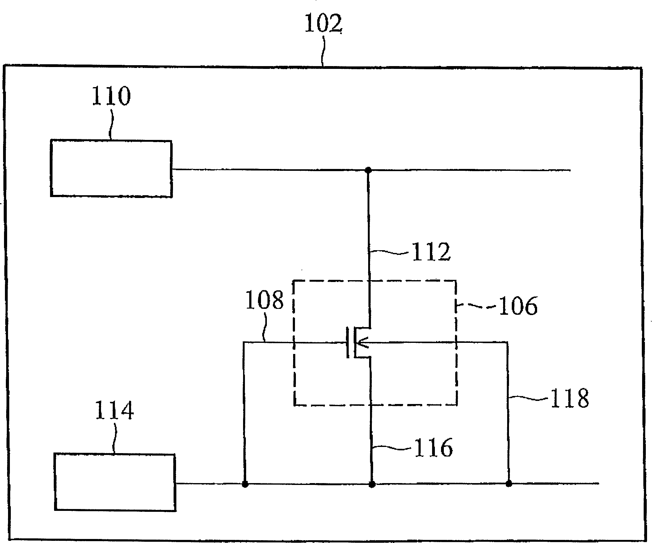
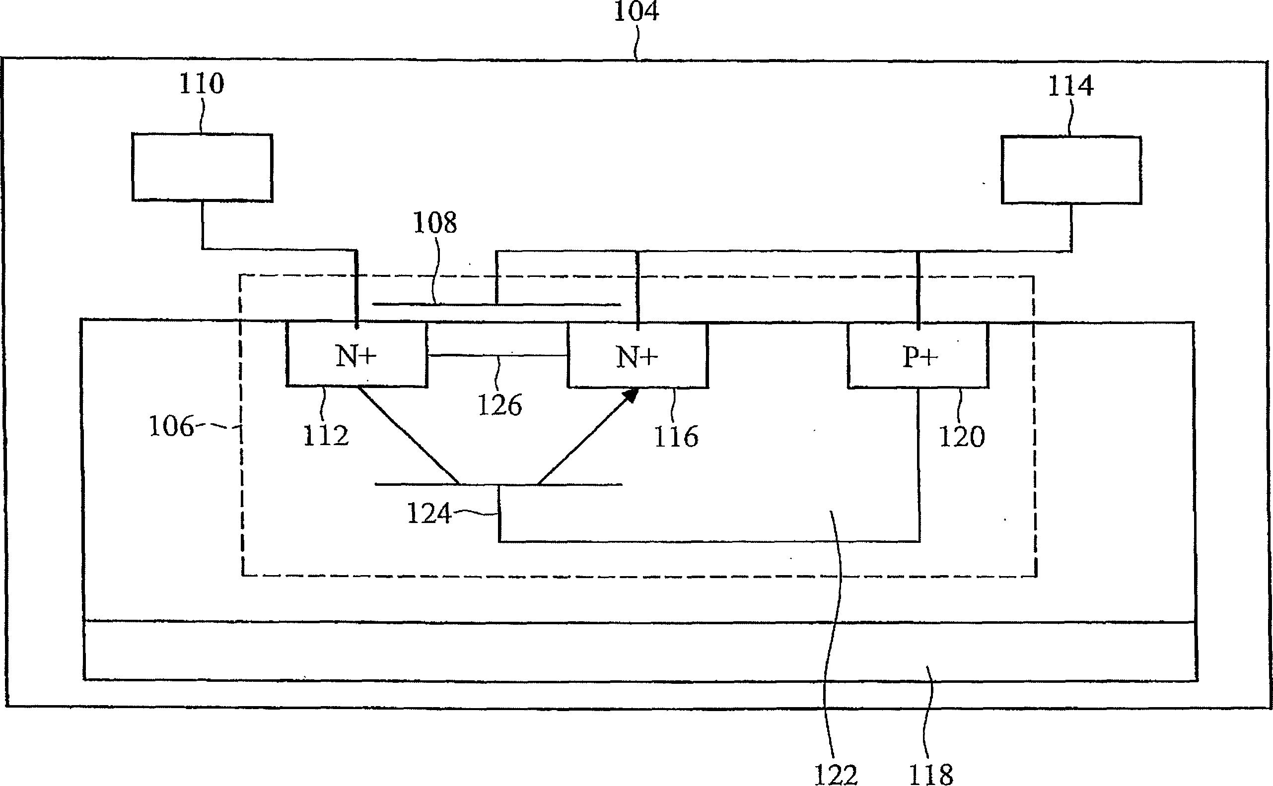
[0039] Figure 3A and Figure 3B According to an embodiment of the present invention, a circuit diagram of an ESD protection circuit 302 and its cross-sectional view 304 are shown. In this embodiment, an NMOS transistor with adjustable trigger voltage is disclosed. Wherein, a voltage differential module, such as a resistor, is placed between the gate of the NMOS transistor and the ground. This resistor comes from a section of the guard ring and can be adjusted by varying its length. Therefore, the resistance value and the bias voltage applied to the NMOS transistor are changed, that is to say, the trigger voltage of the ESD protection circuit is adjustable, and no additional components, photomasks, or layout area are required. This embodiment provides innovative u...


PUM


Abstract

The invention relates to an electrostatic discharge protection circuit comprising: a NMOS transistor and a voltage differentiation module. The NMOS transistor connected between a first pad and a second pad coupled to ground. The voltage differentiation module is connected between a gate of the NMOS transistor and the second pad for creating a bias on the gate during the ESD event, thereby activating a surface current path in addition to a substrate current path for dissipating the ESD current. The voltage differentiation module is formed by a segment of a guard ring, which provides a predefined resistance determining the bias on the gate.

Description

technical field [0001] The present invention relates to a semiconductor circuit, especially an electrostatic discharge (ESD) protection circuit with adjustable trigger voltage. Background technique [0002] Integrated circuits (ICs) are highly susceptible to reliability problems. One of the reliability issues is the possible damage to ICs due to electrostatic discharge (ESD) events. When a charged object, such as a human body with static electricity or a device with a potential different from that of the IC, discharges the static electricity charged to the IC, an electrostatic discharge ESD event will occur. This amount of discharge is typically an amount of current exceeding 1 ampere in 200 nanoseconds. The peak current value and discharge waveform are determined by the equivalent charging resistance, capacitance and inductance of the object subjected to the ESD event. An ESD event typically melts or explodes parts of the IC that are not protected. Therefore, IC designe...

Claims


Application Information

Patent Timeline
IPC IPC(8): H01L23/60H01L27/02H02H9/00
CPCH05K9/0067H01L27/0266H01L29/78
Inventor 黄绍璋
Owner TAIWAN SEMICON MFG CO LTD
Features
  • R&D
  • Intellectual Property
  • Life Sciences
  • Materials
  • Tech Scout
  • Unparalleled Data Quality
  • Higher Quality Content
  • 60% Fewer Hallucinations
Learn More