
Seal ring structure for integrated circuit chips

A sealing ring and semiconductor technology, applied in the direction of semiconductor devices, semiconductor/solid device manufacturing, semiconductor/solid device components, etc.

Active Publication Date: 2006-05-10
TAIWAN SEMICON MFG CO LTD
View PDF0 Cites 33 Cited by
  • Summary
  • Abstract
  • Description
  • Claims
  • Application Information

AI Technical Summary

Problems solved by technology

[0007] Therefore, the plugs in the existing sealing ring structure need to be better designed to limit and prevent the advancement of cracks from the edge of the integrated circuit chip

Method used


Image

  • Seal ring structure for integrated circuit chips
  • Seal ring structure for integrated circuit chips
  • Seal ring structure for integrated circuit chips

Examples


Embodiment Construction

[0047] In order to make the above and other objects, features and advantages of the present invention more comprehensible, a preferred embodiment is specifically cited below, together with the accompanying drawings, and is described in detail as follows:

[0048] The invention discloses a sealing ring structure, which has strong physical strength and includes multiple metallization layers, which can preferably limit and prevent the advancement of cracks. The sealing ring structure is in a region between a core circuit and the edge of an integrated circuit chip and has a thick structure. This structure is a stack formed by upper bridges and lower bridges. Can provide greater mass and strength for improved resistance to crack intrusion.

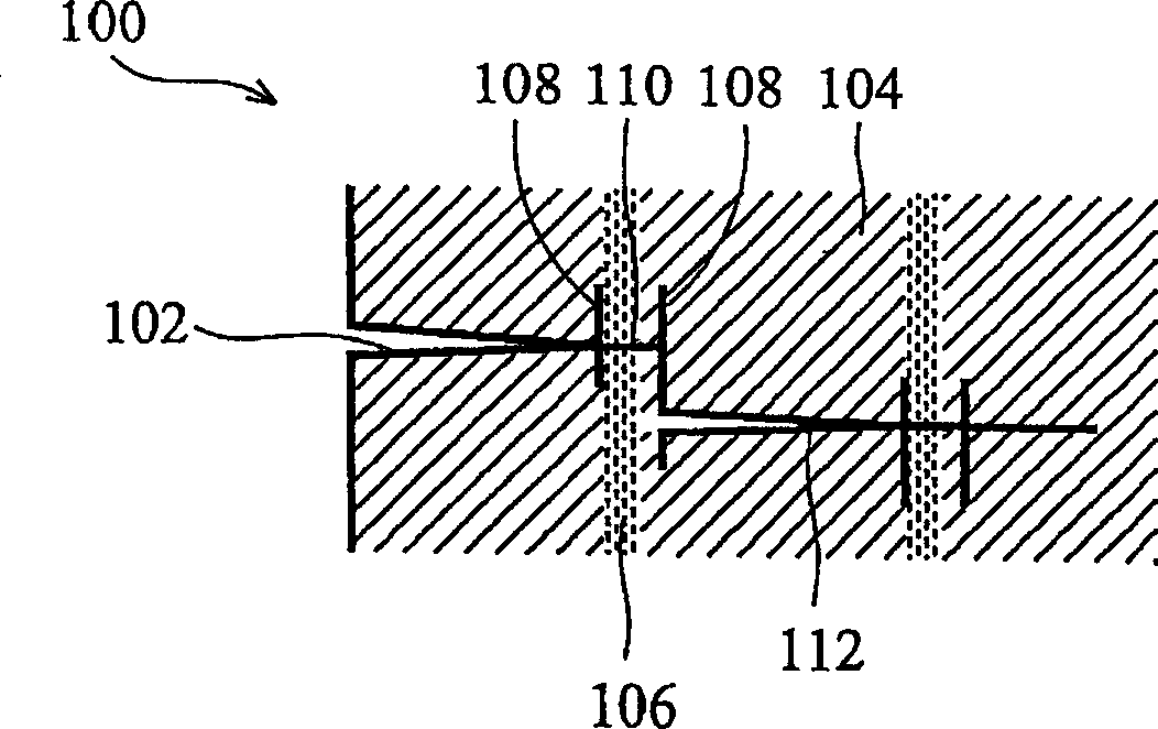
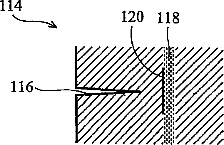
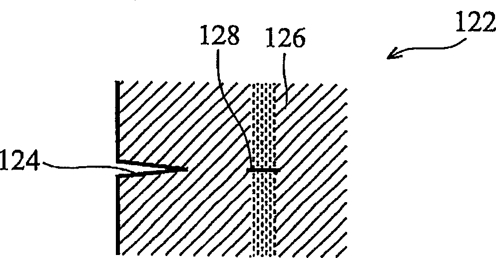
[0049] A common failure situation that an integrated circuit chip may encounter is the generation and propagation of stress cracks from the edge of the integrated circuit chip. Such a failure can be achieved by Figure 1A This is caused by t...


PUM

PropertyMeasurementUnit
widthaaaaaaaaaa
widthaaaaaaaaaa
widthaaaaaaaaaa

Abstract

This invention provides one sealed ring structure, semi-conductor crystal cycle and its method to arouse stress impact, wherein, the structure is suitable for one integration circuit chip core circuit area and comprises the following parts: one metal layer with one bridge layer and one bolt layer, one bridge connection part located the bridge layer between the integration circuit chip periphery and one certain position of the core circuit area; one bolt located in bolt layer aligning to bridge, wherein, the bolt has one width near to bridge. The said sealed ring structure and semi-conductor circle and the method limit crack progression on periphery.

Description

technical field [0001] The present invention relates to the design of semiconductor integrated circuit chips, and more particularly to a sealing ring structure (sealing ring structure), which has sufficient physical strength to limit and prevent the formation of corners and edges of integrated circuit chips. advance of the crack. Background technique [0002] Integrated circuit chips are manufactured in a rectangular array on a circular single crystal wafer. Most wafers are formed from silicon. Wafers can be divided by scribing, breaking, stress breaking or most commonly sawing. The separation line is aligned with the selected crystal axis, so that the separation of the wafers can be performed in a sequence and in a predetermined manner. However, this separation procedure still inevitably results in unintentional stress cracks. Such cracks occur at most near the corners of the integrated circuit chip where two perpendicular dividing lines intersect. Such fractures also ...

Claims


Application Information

Patent Timeline
Patent Type & Authority Applications(China)
IPC IPC(8): H01L23/00H01L27/02
CPCB28D5/0011H01L21/76224H01L21/78H01L23/562H01L23/585H01L2924/0002H01L2924/3011H01L2924/00
Inventor 姚志翔黄泰钧纪冠守郑志成梁明硕万文恺夏劲秋梁孟松
Owner TAIWAN SEMICON MFG CO LTD
Features
  • Generate Ideas
  • Intellectual Property
  • Life Sciences
  • Materials
  • Tech Scout
  • Unparalleled Data Quality
  • Higher Quality Content
  • 60% Fewer Hallucinations
Learn More