

Substrate treating apparatus
A kind of substrate processing equipment and substrate processing technology, applied in the direction of electrical components, semiconductor/solid-state device manufacturing, circuits, etc., can solve the problems of pollution, increased cost, inconvenient installation space, etc., and achieve the goal of shortening the transportation path and effectively conveying Effect
- Summary
- Abstract
- Description
- Claims
- Application Information
AI Technical Summary
Problems solved by technology
Method used
Image

Examples
Embodiment 1
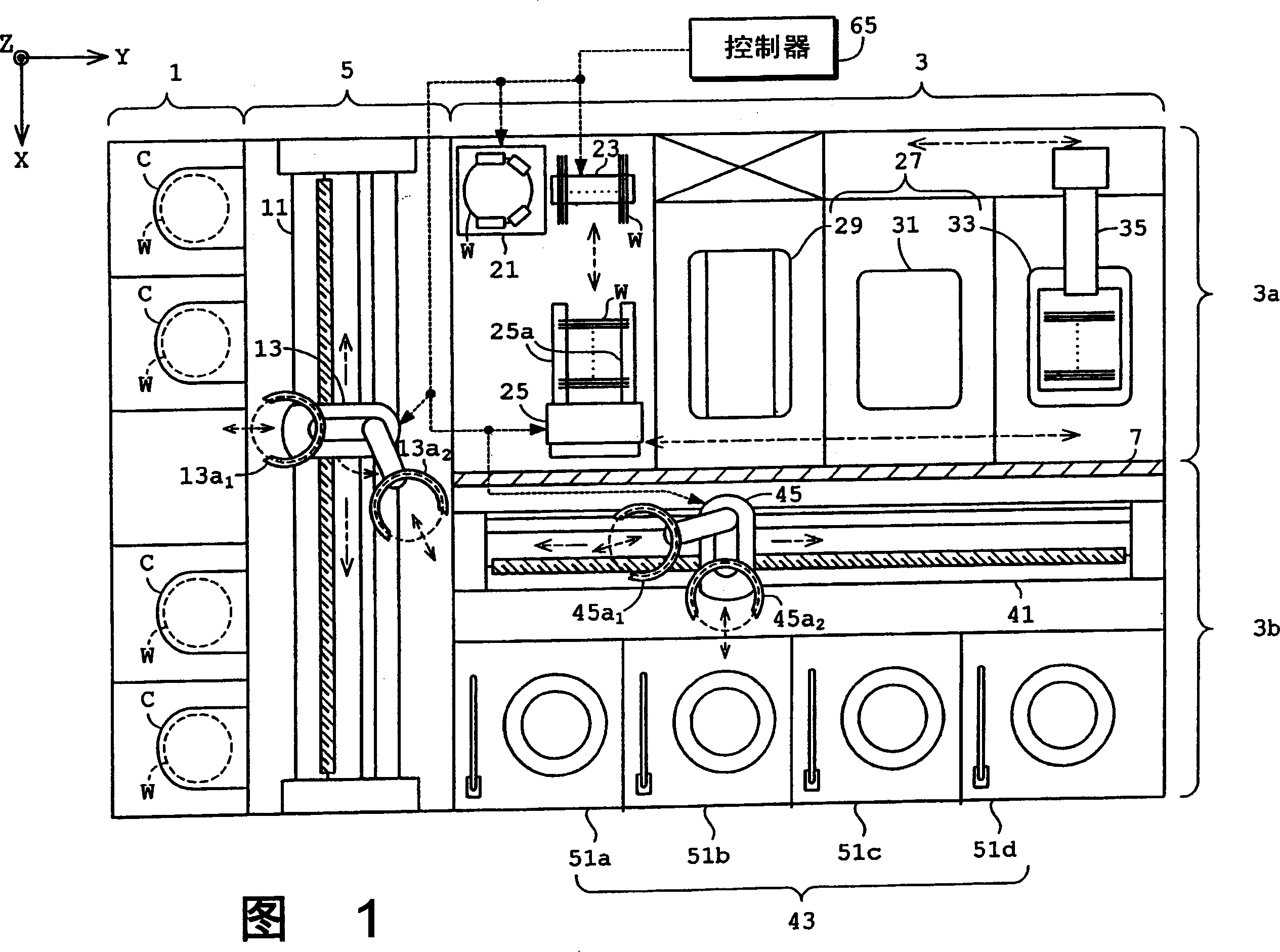
[0136] FIG. 1 is a schematic plan view of a substrate processing apparatus in Embodiment 1. FIG.
[0137] This substrate processing apparatus is configured to perform predetermined processing (eg, protective layer peeling processing) of a substrate or wafer W (eg, semiconductor wafer). The apparatus generally includes a cassette stage 1 for supporting cassettes C storing wafers W, a processing area 3 for performing predetermined processing of wafers W, and a transport for transferring wafers W provided between cassette table 1 and processing area 3. District 5. The processing block 3 has a first processing section 3a for processing many wafers W as a whole and a second processing section 3b for processing one wafer W at a time.
[0138] Each cassette C placed on the cassette stage 1 contains many (for example, 25) wafers W in a horizontal state and in multiple layers (hereinafter, many wafers W may be referred to as a group of wafers W where appropriate).
[0139] The transp...
Embodiment 2
[0196] Next, Embodiment 2 of the present invention will be described.
[0197] FIG. 9 is a schematic plan view of a substrate processing apparatus in Embodiment 2. FIG. The same reference numerals are used for the same parts as those in Embodiment 1, and their further descriptions are omitted.
[0198] The substrate processing apparatus in Embodiment 2 generally includes a cassette table 1 , a processing area 3 , a transport area 5 and an auxiliary transport area 9 . The auxiliary conveying zone 9 is arranged across the processing zone 3 opposite to the conveying zone 5 .
[0199] The auxiliary transfer area 9 is provided therein with a transfer mechanism 45 for transferring the wafer W to the second processing section and a second posture for receiving the wafer from the mechanism and changing the posture of the entire group of wafers between the horizontal posture and the vertical posture. A changer 61, a transfer mechanism 26 for transferring the group of wafers W to a fi...
Embodiment 3
[0221] Next, Embodiment 3 of the present invention will be described with reference to the drawings.
[0222] Figure 10 is a schematic plan view of the substrate processing apparatus in Embodiment 3.
[0223]The substrate processing apparatus in Embodiment 3 is designed to clean, etch and dry a wafer W (such as a semiconductor wafer), and includes containers for receiving seals (called FOUPs (Front Opening Unitary Containers), hereinafter Each container is used to store a plurality of wafers W, and includes a first processing area 103 for processing all of the plurality of wafers W, and a first processing area 103 for processing one wafer W at a time. A second processing area 105 , and a transfer area 107 for transferring the wafer W between the storage area 101 , the first processing area 103 and the second processing area 105 . Each integral container F corresponds to a container in the present invention. The storage area 101 , the first processing area 103 , the second ...
PUM
 Abstract
Description
Claims
Application Information