
Logic gate with a potential-free gate electrode for organic integrated circuits

A logic gate, organic technology, applied in logic circuits using specific components, logic circuits, circuits using semiconductor devices, etc., to achieve the effect of improving conversion properties, rapid and stable conversion or action, and space needs to be improved

Inactive Publication Date: 2012-01-25
POLYIC GMBH & CO KG
View PDF3 Cites 0 Cited by
  • Summary
  • Abstract
  • Description
  • Claims
  • Application Information

AI Technical Summary

Problems solved by technology

[0004]An organic logic gate circuit capable of switching quickly and stably even with low supply voltages has not yet been realized

Method used


Image

  • Logic gate with a potential-free gate electrode for organic integrated circuits
  • Logic gate with a potential-free gate electrode for organic integrated circuits
  • Logic gate with a potential-free gate electrode for organic integrated circuits

Examples


Embodiment Construction

[0022] The same reference numerals are used for the same or similar elements in the specification and drawings.

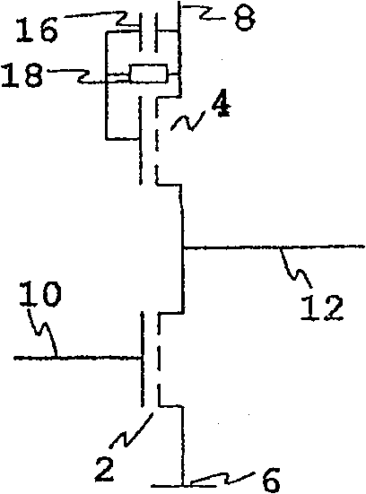
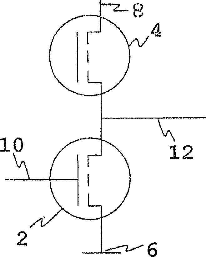
[0023] figure 1 One embodiment of a logic gate using a charge FET with a potential-free gate is illustrated. The selected logic gates are here embodied as inverters because the advantages of the invention are most clearly illustrated by inverters being the simplest components. figure 1 Two transistors 2 and 4 are shown connected in series to form an inverter. In this case, transistor 2 is a switching transistor and transistor 4 is a charging transistor. exist figure 1 , the source 6 of the switching FET 2 is grounded. The drain is connected to the output 12 of the inverter. The gate 10 of the switching transistor 2 forms the input of the inverter. The source and drain of the charging transistor 4 connect the output 12 of the inverter to the supply voltage 8 .

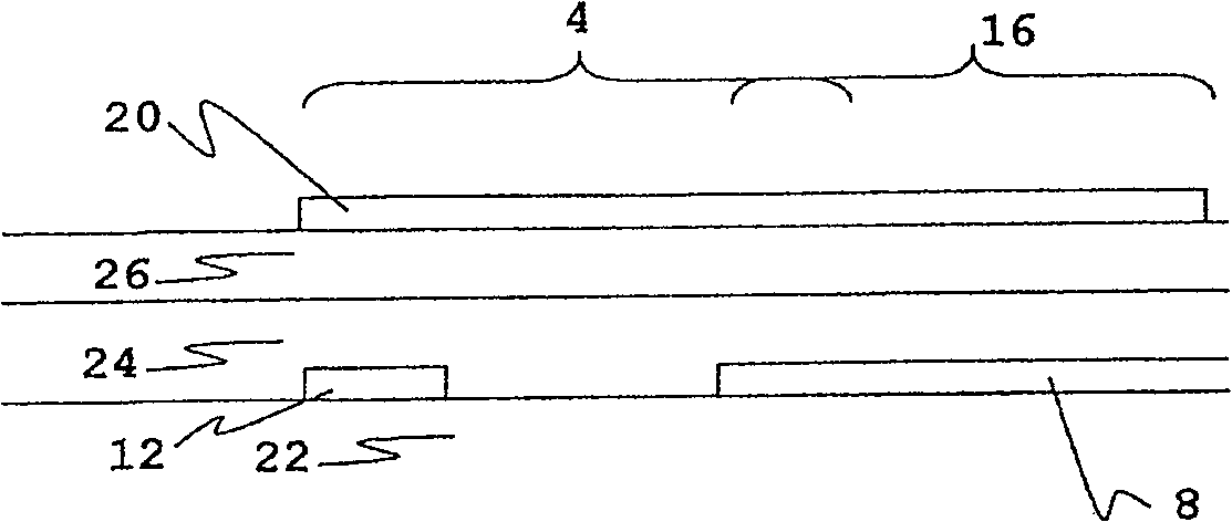
[0024] figure 2 One embodiment of an inverter using a charge FET with a gate capacitively cou...


PUM


Abstract

The invention relates to an organic logic gate comprising at least one charging field effect transistor (charging FET) and at least one switching field effect transistor (switching FET), the charging FET having at least one gate electrode, a source electrode and a drain electrode, the gate electrode of the charging FET being potential-free.

Description

technical field [0001] The technical field of the invention relates to organic logic gates, such as AND, NAND, NOR, and the like. The invention also addresses the issues of switching times and switching stability of organic logic gates. Background technique [0002] This problem has hitherto been only partly solved by connecting the gates of charging field effect transistors (FETs) in logic gates to the supply voltage, whereby fast logic gates can be provided. However, this solution requires a high supply voltage greater than 20V. For example, in the article "Fast polymer integrated circuits" in Applied Physics Letters, Issue 81, page 1735 (2002) in "Applied Physics Letters", Issue 81, page 1735 (2002) Such a measure for improving the switching behavior of organic logic gates is described. [0003] "High performance all-polymer integrated circuits" in Applied Physics Letters, Issue 77, page 1487 (2000) in the article "High performance all-polymer integrated circuits" in ...

Claims


Application Information

Patent Timeline
Patent Type & Authority Patents(China)
IPC IPC(8): H01L27/00H03K19/08H03K19/094H03K19/02H01L27/28
CPCH03K19/094H01L27/28H10K19/80H10K19/00
Inventor 沃尔弗拉姆·格劳尔特沃尔特·菲克斯安德烈亚斯·厄尔曼
Owner POLYIC GMBH & CO KG
Learn More